参数资料
| 型号: | LTC1555CGN#PBF |
| 厂商: | Linear Technology |
| 文件页数: | 11/12页 |
| 文件大小: | 0K |
| 描述: | IC LEVEL TRANSLATOR 16-SSOP |
| 标准包装: | 100 |
| 逻辑功能: | 电平移位器 |
| 位数: | 1 |
| 输入类型: | 电压 |
| 输出类型: | 电压 |
| 通道数: | 1 |
| 输出/通道数目: | 1 |
| 差分 - 输入:输出: | 无/无 |
| 传输延迟(最大): | 18ns |
| 电源电压: | 1.8 V ~ 5.5 V |
| 工作温度: | 0°C ~ 70°C |
| 封装/外壳: | 16-SSOP(0.154",3.90mm 宽) |
| 供应商设备封装: | 16-SSOP |
| 包装: | 管件 |
8
LTC1555/LTC1556
APPLICATIONS INFORMATION
WU
U
reduce the ripple. A larger COUT capacitor (22F or greater)
will reduce both the low and high frequency ripple due to
the lower COUT charging and discharging dV/dt and the
lower ESR typically found with higher value (larger case
size) capacitors. A low ESR ceramic output capacitor will
minimize the high frequency ripple, but will not reduce the
low frequency ripple unless a high capacitance value is
chosen (10
F or greater). A reasonable compromise is to
use a 10
Fto22Ftantalumcapacitorinparallelwitha1F
to 3.3
F ceramic capacitor on VOUT to reduce both the low
and high frequency ripple. An RC filter may also be used
to reduce high frequency voltage spikes (see Figure 1).
hundred milliseconds to completely shut down. To ensure
prompt and proper VCC shutdown, always force the M0
and M1 pins to a logic low state before shutting down the
DVCC supply (see Figure 2). Similarly, bring the DVCC
supply to a valid level before allowing the M0 and M1 pins
to go high when coming out of shutdown. This can be
achieved with pull-down resistors from M0 and M1 to
GND if necessary. (Note: shutting down the DVCC supply
with VIN active is not recommended with early date code
material. Consult factory for valid date code starting point
for shutting down the DVCC supply.)
Level Translators
All SIMs and smart cards contain a clock input, reset input
and a bidirectional data input/output. The LTC1555/
LTC1556 provide level translators to allow controllers to
communicate with the SIM (see Figures 3a and 3b). The
CLK and RST inputs to the SIM are level shifted from the
controller supply rails (DVCC and GND) to the SIM supply
rails (VCC and GND). The data input to the SIM may be
provided two different ways. The first method is to use the
DATA pin as a bidirectional level translator. This configu-
ration is only allowed if the controller data output pin is
open drain (all SIM I/O pins are open drain). Internal pull-
up resistors are provided for both the DATA pin and the
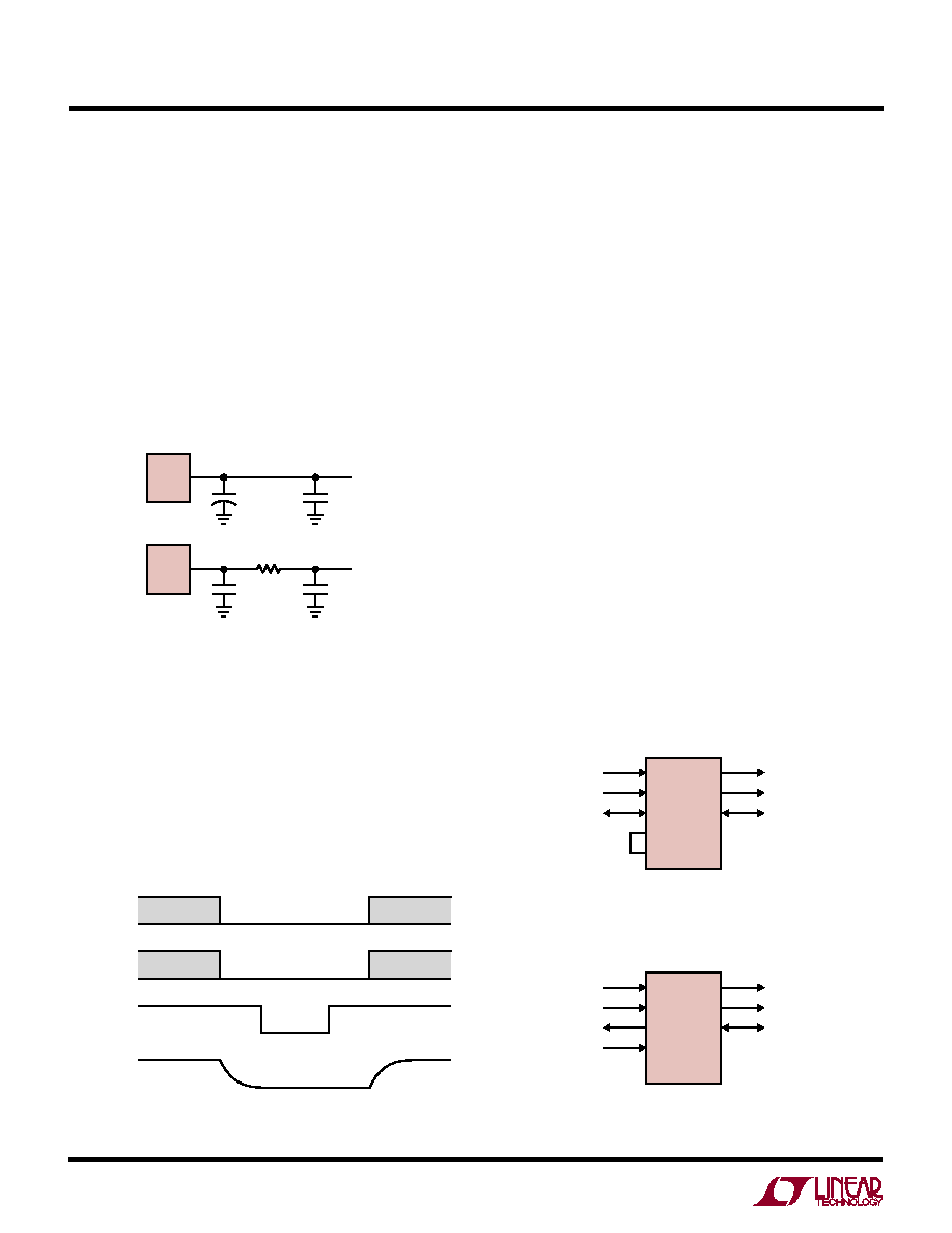
Figure 3b. Level Translator Connections for
One-Directional Controller Side DATA Flow
CIN
RIN
DATA
DDRV
DVCC
CLK
RST
I/O
VCC
CLK TO SIM
RST TO SIM
DATA FROM SIM
DATA TO SIM
LTC1555/LTC1556
CONTROLLER
SIDE
SIM SIDE
1555/56 F3b
Figure 3a. Level Translator Connections for
Bidirectional Controller DATA Pin
CIN
RIN
DATA
DDRV
DVCC
CLK
RST
I/O
VCC
CLK TO SIM
RST TO SIM
DATA TO/FROM SIM
LTC1555/LTC1556
CONTROLLER
SIDE
SIM SIDE
1555/56 F3a
Figure 2. Recommended DVCC Shutdown and Start-Up Timing
M0
DVCC
0V
M1
DVCC
0V
DVCC
0V
VCC
0V
1555/56 F02
Shutting Down the DVCC Supply
To conserve power, the DVCC supply may be shut down
while the VIN supply is still active. When the DVCC supply
is brought to 0V, weak internal currents will force the
LTC1555/LTC1556 into shutdown mode regardless of the
voltages present on the M0 and M1 pins. However, if the
M0 and M1 pins are floating or left connected to DVCC as
the supply is shut down, the parts may take several
Figure 1. VCC Output Ripple Reduction Techniques
15
F
TANTALUM
LT1555/56 F01
VCC
SIM
VCC
SIM
VCC
1
F
CERAMIC
10
F
VCC
10
F
2
LTC1555/
LTC1556
+
相关PDF资料 |
PDF描述 |
|---|---|
| V24B6V5M200BF | CONVERTER MOD DC/DC 6.5V 200W |
| MS27467T17F99PLC | CONN HSG PLUG 23POS STRGHT PINS |
| MS27468T11A35PLC | CONN HSG RCPT 13POS JAM NUT PIN |
| V24B6V5M200BL2 | CONVERTER MOD DC/DC 6.5V 200W |
| MS27467T19F35SLC | CONN HSG PLUG 66POS STRGHT SCKT |
相关代理商/技术参数 |
参数描述 |
|---|---|
| LTC1555IGN | 功能描述:IC LEVEL TRANSLATOR 16-SSOP RoHS:否 类别:集成电路 (IC) >> 逻辑 - 变换器 系列:- 产品培训模块:Logic Packages 标准包装:2,500 系列:- 逻辑功能:变换器,双向 位数:2 输入类型:电压 输出类型:电压 数据速率:- 通道数:2 输出/通道数目:1 差分 - 输入:输出:无/无 传输延迟(最大):1.5ns 电源电压:3 V ~ 3.6 V 工作温度:-40°C ~ 85°C 封装/外壳:8-TSSOP,8-MSOP(0.118",3.00mm 宽) 供应商设备封装:8-TSSOP 包装:带卷 (TR) 其它名称:935284857118GTL2002DP/S440-TGTL2002DP/S440-T-ND |
| LTC1555IGN#PBF | 功能描述:IC LEVEL TRANSLATOR 16-SSOP RoHS:是 类别:集成电路 (IC) >> 逻辑 - 变换器 系列:- 标准包装:1 系列:100ELT 逻辑功能:变换器 位数:1 输入类型:TTL 输出类型:差分 数据速率:- 通道数:2 输出/通道数目:1 差分 - 输入:输出:无/是 传输延迟(最大):0.6ns 电源电压:3 V ~ 3.8 V 工作温度:-40°C ~ 85°C 封装/外壳:8-SOIC(0.154",3.90mm 宽) 供应商设备封装:8-SOIC 包装:Digi-Reel® 产品目录页面:1088 (CN2011-ZH PDF) 其它名称:576-1360-6 |
| LTC1555IGN#TR | 功能描述:IC LEVEL XLATOR/SIM PS 16SSOP RoHS:否 类别:集成电路 (IC) >> 逻辑 - 变换器 系列:- 产品培训模块:Logic Packages 标准包装:2,500 系列:- 逻辑功能:变换器,双向 位数:2 输入类型:电压 输出类型:电压 数据速率:- 通道数:2 输出/通道数目:1 差分 - 输入:输出:无/无 传输延迟(最大):1.5ns 电源电压:3 V ~ 3.6 V 工作温度:-40°C ~ 85°C 封装/外壳:8-TSSOP,8-MSOP(0.118",3.00mm 宽) 供应商设备封装:8-TSSOP 包装:带卷 (TR) 其它名称:935284857118GTL2002DP/S440-TGTL2002DP/S440-T-ND |
| LTC1555IGN#TRPBF | 功能描述:IC LEVEL TRANSLATOR 16-SSOP RoHS:是 类别:集成电路 (IC) >> 逻辑 - 变换器 系列:- 产品培训模块:Logic Packages 标准包装:2,500 系列:- 逻辑功能:变换器,双向 位数:2 输入类型:电压 输出类型:电压 数据速率:- 通道数:2 输出/通道数目:1 差分 - 输入:输出:无/无 传输延迟(最大):1.5ns 电源电压:3 V ~ 3.6 V 工作温度:-40°C ~ 85°C 封装/外壳:8-TSSOP,8-MSOP(0.118",3.00mm 宽) 供应商设备封装:8-TSSOP 包装:带卷 (TR) 其它名称:935284857118GTL2002DP/S440-TGTL2002DP/S440-T-ND |
| LTC1555LEGN | 功能描述:IC LEVEL TRANSLATER 16-SSOP RoHS:否 类别:集成电路 (IC) >> 逻辑 - 变换器 系列:- 产品培训模块:Logic Packages 标准包装:2,500 系列:- 逻辑功能:变换器,双向 位数:2 输入类型:电压 输出类型:电压 数据速率:- 通道数:2 输出/通道数目:1 差分 - 输入:输出:无/无 传输延迟(最大):1.5ns 电源电压:3 V ~ 3.6 V 工作温度:-40°C ~ 85°C 封装/外壳:8-TSSOP,8-MSOP(0.118",3.00mm 宽) 供应商设备封装:8-TSSOP 包装:带卷 (TR) 其它名称:935284857118GTL2002DP/S440-TGTL2002DP/S440-T-ND |
发布紧急采购,3分钟左右您将得到回复。