- 您现在的位置:买卖IC网 > PDF目录11030 > LTC1563-3IGN (Linear Technology)IC FILTER LP RC 4TH ORDER 16SSOP PDF资料下载
参数资料
| 型号: | LTC1563-3IGN |
| 厂商: | Linear Technology |
| 文件页数: | 3/20页 |
| 文件大小: | 0K |
| 描述: | IC FILTER LP RC 4TH ORDER 16SSOP |
| 标准包装: | 100 |
| 滤波器类型: | 巴特沃斯,低通开关电容器 |
| 频率 - 截止或中心: | 256kHz |
| 滤波器数: | 1 |
| 滤波器阶数: | 4th |
| 电源电压: | 2.7 V ~ 11 V,±2.7 V ~ 5.5 V |
| 安装类型: | 表面贴装 |
| 封装/外壳: | 16-SSOP(0.154",3.90mm 宽) |
| 供应商设备封装: | 16-SSOP |
| 包装: | 管件 |
11
LTC1563-2/LTC1563-3
156323fa
APPLICATIONS INFORMATION
WU
U
Output Loading: Resistive and Capacitive
The op amps of the LTC1563-X have a rail-to-rail output
stage. To obtain maximum performance, the output load-
ing effects must be considered. Output loading issues can
be divided into resistive effects and capacitive effects.
Resistive loading affects the maximum output signal swing
and signal distortion. If the output load is excessive, the
output swing is reduced and distortion is increased. All of
the output voltage swing testing on the LTC1563-X is done
with R22 = 100k and a 10k load resistor. For best undistorted
output swing, the output load resistance should be greater
than 10k.
Capacitive loading on the output reduces the stability of
the op amp. If the capacitive loading is sufficiently high,
the stability margin is decreased to the point of oscillation
at the output. Capacitive loading should be kept below
30pF. Good, tight layout techniques should be maintained
at all times. These parts should not drive long traces and
must never drive a long coaxial cable.
When probing the
LTC1563-X, always use a 10x probe. Never use a 1x probe.
A standard 10x probe has a capacitance of 10pF to 15pF
while a 1x probe’s capacitance can be as high as 150pF.
The use of a 1x probe will probably cause oscillation.
For larger capacitive loads, a series isolation resistor can
be used between the part and the capacitive load. If the
load is too great, a buffer must be used.
Layout Precautions
The LTC1563-X is an active RC filter. The response of the
filter is determined by the on-chip capacitors and the
external resistors. Any external, stray capacitance in par-
allel with an on-chip capacitor, or to an AC ground, can
alter the transfer function.
Capacitance to an AC ground is the most likely problem.
Capacitance on the LPA or LPB pins does not affect the
transfer function but does affect the stability of the op
amps. Capacitance on the INVA and INVB pins will affect
the transfer function somewhat and will also affect the
stability of the op amps. Capacitance on the SA and SB
pins alters the transfer function of the filter. These pins are
the most sensitive to stray capacitance. Stray capacitance
on these pins results in peaking of the frequency response
near the cutoff frequency. Poor layout can give 0.5dB to
1dB of excess peaking.
To minimize the effects of parasitic layout capacitance, all
of the resistors for section A should be placed as close as
possible to the SA pin. Place the R31 resistor first so that
it is as close as possible to the SA pin on one end and as
close as possible to the INVA pin on the other end. Use the
same strategy for the layout of section B, keeping all of the
resistors as close as possible to the SB node and first
placing R32 between the SB and INVB pins. It is also best
if the signal routing and resistors are on the same layer as
the part without any vias in the signal path.
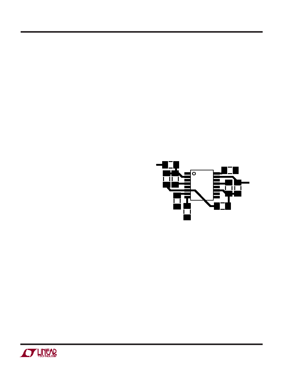
Figure 1 illustrates a good layout using the LTC1563-X
with surface mount 0805 size resistors. An even tighter
layout is possible with smaller resistors.
1653 F01
R11
LTC1563-X
R12
R32
R22
R21
R31
VOUT
VIN
Figure 1. PC Board Layout
Single Pole Sections and Odd Order Filters
The LTC1563 is configured to naturally form even ordered
filters (2nd, 4th, 6th and 8th). With a little bit of work,
single pole sections and odd order filters are easily achieved.
To form a single pole section you simply use the op amp,
the on-chip C1 capacitor and two external resistors as
shown in Figure 2. This gives an inverting section with the
gain set by the R2-R1 ratio and the pole set by the R2-C1
time constant. You can use this pole with a 2nd order
section to form a noninverting gain 3rd order filter or as a
stand alone inverting gain single pole filter.
Figure 3 illustrates another way of making odd order
filters. The R1 input resistor is split into two parts with an
additional capacitor connected to ground in between the
resistors. This “TEE” network forms a single real pole. RB1
相关PDF资料 |
PDF描述 |
|---|---|
| VI-J4J-IW-B1 | CONVERTER MOD DC/DC 36V 100W |
| VI-J42-IW-B1 | CONVERTER MOD DC/DC 15V 100W |
| LTC1563-2IGN | IC FILTER LP RC 4TH ORDER 16SSOP |
| VI-J41-IW-B1 | CONVERTER MOD DC/DC 12V 100W |
| VE-JT1-IW-B1 | CONVERTER MOD DC/DC 12V 100W |
相关代理商/技术参数 |
参数描述 |
|---|---|
| LTC1563-3IGN#PBF | 功能描述:IC FILTER LP RC 4TH ORDER 16SSOP RoHS:是 类别:集成电路 (IC) >> 接口 - 滤波器 - 有源 系列:- 产品培训模块:Lead (SnPb) Finish for COTS Obsolescence Mitigation Program 标准包装:1,000 系列:- 滤波器类型:连续时间,带通低通 频率 - 截止或中心:150kHz 滤波器数:4 滤波器阶数:8th 电源电压:4.74 V ~ 11 V,±2.37 V ~ 5.5 V 安装类型:表面贴装 封装/外壳:28-SOIC(0.295",7.50mm 宽) 供应商设备封装:28-SOIC W 包装:带卷 (TR) |
| LTC1563-3IGN#TR | 功能描述:IC FILTER LP RC 4TH ORDER 16SSOP RoHS:否 类别:集成电路 (IC) >> 接口 - 滤波器 - 有源 系列:- 产品培训模块:Lead (SnPb) Finish for COTS Obsolescence Mitigation Program 标准包装:1,000 系列:- 滤波器类型:连续时间,带通低通 频率 - 截止或中心:150kHz 滤波器数:4 滤波器阶数:8th 电源电压:4.74 V ~ 11 V,±2.37 V ~ 5.5 V 安装类型:表面贴装 封装/外壳:28-SOIC(0.295",7.50mm 宽) 供应商设备封装:28-SOIC W 包装:带卷 (TR) |
| LTC1563-3IGN#TRPBF | 功能描述:IC FILTER LP RC 4TH ORDER 16SSOP RoHS:是 类别:集成电路 (IC) >> 接口 - 滤波器 - 有源 系列:- 产品培训模块:Lead (SnPb) Finish for COTS Obsolescence Mitigation Program 标准包装:1,000 系列:- 滤波器类型:连续时间,带通低通 频率 - 截止或中心:150kHz 滤波器数:4 滤波器阶数:8th 电源电压:4.74 V ~ 11 V,±2.37 V ~ 5.5 V 安装类型:表面贴装 封装/外壳:28-SOIC(0.295",7.50mm 宽) 供应商设备封装:28-SOIC W 包装:带卷 (TR) |
| LTC1564CG | 功能描述:IC ANTIALIASING FILTER 16-SSOP RoHS:否 类别:集成电路 (IC) >> 接口 - 滤波器 - 有源 系列:- 产品培训模块:Lead (SnPb) Finish for COTS Obsolescence Mitigation Program 标准包装:1,000 系列:- 滤波器类型:连续时间,带通低通 频率 - 截止或中心:150kHz 滤波器数:4 滤波器阶数:8th 电源电压:4.74 V ~ 11 V,±2.37 V ~ 5.5 V 安装类型:表面贴装 封装/外壳:28-SOIC(0.295",7.50mm 宽) 供应商设备封装:28-SOIC W 包装:带卷 (TR) |
| LTC1564CG#PBF | 功能描述:IC ANTIALIASING FILTER 16-SSOP RoHS:是 类别:集成电路 (IC) >> 接口 - 滤波器 - 有源 系列:- 产品培训模块:Lead (SnPb) Finish for COTS Obsolescence Mitigation Program 标准包装:1,000 系列:- 滤波器类型:连续时间,带通低通 频率 - 截止或中心:150kHz 滤波器数:4 滤波器阶数:8th 电源电压:4.74 V ~ 11 V,±2.37 V ~ 5.5 V 安装类型:表面贴装 封装/外壳:28-SOIC(0.295",7.50mm 宽) 供应商设备封装:28-SOIC W 包装:带卷 (TR) |
发布紧急采购,3分钟左右您将得到回复。