- 您现在的位置:买卖IC网 > PDF目录11025 > LTC1569IS8-7#TR (Linear Technology)IC FILTER LP 10TH ORD LIN 8SOIC PDF资料下载
参数资料
| 型号: | LTC1569IS8-7#TR |
| 厂商: | Linear Technology |
| 文件页数: | 11/12页 |
| 文件大小: | 0K |
| 描述: | IC FILTER LP 10TH ORD LIN 8SOIC |
| 标准包装: | 2,500 |
| 滤波器类型: | 线性相位,低通开关电容器 |
| 频率 - 截止或中心: | 300kHz |
| 滤波器数: | 1 |
| 滤波器阶数: | 10th |
| 安装类型: | 表面贴装 |
| 封装/外壳: | 8-SOIC(0.154",3.90mm 宽) |
| 供应商设备封装: | 8-SOIC |
| 包装: | 带卷 (TR) |
8
LTC1569-7
input signal at IN + should be centered around the DC
voltage at IN –. The input can also be AC coupled, as shown
in the Typical Applications section.
For inverting single-ended filtering, connect IN+ to GND or
to quiet DC reference voltage. Apply the signal to IN –. The
DC gain from IN – to OUT is –1, assuming IN – is referenced
to IN + and OUT is reference to GND.
Refer to the Typical Performance Characteristics section
to estimate the THD for a given input level.
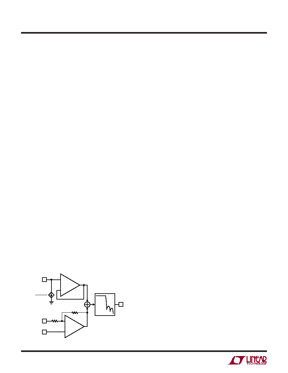
Dynamic Input Impedance
The unique input sampling structure of the LTC1569-7 has
a dynamic input impedance which depends on the con-
figuration, i.e., differential or single-ended, and the clock
frequency. The equivalent circuit in Figure 8 illustrates the
input impedance when the cutoff frequency is 128kHz. For
other cutoff frequencies replace the 125k value with
125k (128kHz/fCUTOFF).
When driven with a single-ended signal into IN – with IN +
tied to GND, the input impedance is very high (~10M
).
When driven with a single-ended signal into IN + with IN –
tied to GND, the input impedance is a 125k resistor to GND.
When driven with a complementary signal whose com-
mon mode voltage is GND, the IN+ input appears to have
125k to GND and the IN – input appears to have –125k to
GND. To make the effective IN – impedance 125k when
driven differentially, place a 62.5k resistor from IN – to
GND. For other cutoff frequencies use 62.5k (128kHz/
fCUTOFF), as shown in the Typical Applications section. The
typical variation in dynamic input impedance for a given
clock frequency is
±10%.
Wideband Noise
The wideband noise of the filter is the RMS value of the
device’s output noise spectral density. The wideband
noise data is used to determine the operating signal-to-
noise at a given distortion level. The wideband noise is
nearly independent of the value of the clock frequency and
excludes the clock feedthrough. Most of the wideband
noise is concentrated in the filter passband and cannot be
removed with post filtering (Table 2). Table 3 lists the
typical wideband noise for each supply.
APPLICATIONS INFORMATION
WU
U
The oscillator is sensitive to transients on the positive
supply. The IC should be soldered to the PC board and the
PCB layout should include a 1
F ceramic capacitor be-
tween V + (Pin 7) and V – (Pin 4) , as close as possible to
the IC to minimize inductance. Avoid parasitic capacitance
on RX and avoid routing noisy signals near RX (Pin 6). Use
a ground plane connected to V – (Pin 4) for single supply
applications. Connect a ground plane to GND (Pin 3) for
dual supply applications and connect V – (Pin 4) to a
copper trace with low thermal resistance.
Input and Output Range
The input signal range includes the full power supply
range. The output voltage range is typically (V – + 50mV)
to (V + – 0.8V) when VS = 3V. To maximize the undistorted
peak-to-peak signal swing of the filter, the GND (Pin 3)
voltage should be set to 2V (1.11V) in single 5V (3V)
supply applications.
The LTC1569-7 can be driven with a single-ended or
differential signal. When driven differentially, the voltage
between IN + and IN – (Pin 1 and Pin 2) is filtered with a DC
gain of 1. The single-ended output voltage OUT (Pin 8) is
referenced to the voltage of the GND (Pin 3). The common
mode voltage of IN + and IN – can be any voltage that keeps
the input signals within the power supply range.
For noninverting single-ended applications, connect IN –
to GND or to a quiet DC reference voltage and apply the
input signal to IN +. If the input is DC coupled then the DC
gain from IN + to OUT will be 1. This is true given IN + and
OUT are referenced to the same voltage, i.e., GND, V – or
some other DC reference. To achieve the distortion levels
shown in the Typical Performance Characteristics the
Figure 8
8
3
1
2
OUT
IN–
IN+
GND
1569-7 F08
125k
+
–
+
125k
i =
IN+ – GND
125k
相关PDF资料 |
PDF描述 |
|---|---|
| VE-B1Z-IW-F1 | CONVERTER MOD DC/DC 2V 40W |
| VI-J6W-IW-B1 | CONVERTER MOD DC/DC 5.5V 100W |
| LTC1569IS8-7 | IC FILTER LP 10TH ORD LIN 8SOIC |
| VE-B1Y-IY-F3 | CONVERTER MOD DC/DC 3.3V 33W |
| LTC1569IS8-7#PBF | IC FILTER 10TH ORDR LOWPASS8SOIC |
相关代理商/技术参数 |
参数描述 |
|---|---|
| LTC1574CS | 功能描述:IC REG BUCK INV ADJ 16SOIC RoHS:否 类别:集成电路 (IC) >> PMIC - 稳压器 - DC DC 开关稳压器 系列:- 设计资源:Design Support Tool 标准包装:1 系列:- 类型:升压(升压) 输出类型:固定 输出数:1 输出电压:3V 输入电压:0.75 V ~ 2 V PWM 型:- 频率 - 开关:- 电流 - 输出:100mA 同步整流器:是 工作温度:-40°C ~ 85°C 安装类型:表面贴装 封装/外壳:SOT-23-5 细型,TSOT-23-5 包装:剪切带 (CT) 供应商设备封装:TSOT-23-5 其它名称:AS1323-BTTT-30CT |
| LTC1574CS#PBF | 功能描述:IC REG BUCK INV ADJ 16SOIC RoHS:是 类别:集成电路 (IC) >> PMIC - 稳压器 - DC DC 开关稳压器 系列:- 标准包装:250 系列:- 类型:降压(降压) 输出类型:固定 输出数:1 输出电压:1.2V 输入电压:2.05 V ~ 6 V PWM 型:电压模式 频率 - 开关:2MHz 电流 - 输出:500mA 同步整流器:是 工作温度:-40°C ~ 85°C 安装类型:表面贴装 封装/外壳:6-UFDFN 包装:带卷 (TR) 供应商设备封装:6-SON(1.45x1) 产品目录页面:1032 (CN2011-ZH PDF) 其它名称:296-25628-2 |
| LTC1574CS#TR | 功能描述:IC REG BUCK INV ADJ 16SOIC RoHS:否 类别:集成电路 (IC) >> PMIC - 稳压器 - DC DC 开关稳压器 系列:- 设计资源:Design Support Tool 标准包装:1 系列:- 类型:升压(升压) 输出类型:固定 输出数:1 输出电压:3V 输入电压:0.75 V ~ 2 V PWM 型:- 频率 - 开关:- 电流 - 输出:100mA 同步整流器:是 工作温度:-40°C ~ 85°C 安装类型:表面贴装 封装/外壳:SOT-23-5 细型,TSOT-23-5 包装:剪切带 (CT) 供应商设备封装:TSOT-23-5 其它名称:AS1323-BTTT-30CT |
| LTC1574CS#TRPBF | 功能描述:IC REG BUCK INV ADJ 16SOIC RoHS:是 类别:集成电路 (IC) >> PMIC - 稳压器 - DC DC 开关稳压器 系列:- 设计资源:Design Support Tool 标准包装:1 系列:- 类型:升压(升压) 输出类型:固定 输出数:1 输出电压:3V 输入电压:0.75 V ~ 2 V PWM 型:- 频率 - 开关:- 电流 - 输出:100mA 同步整流器:是 工作温度:-40°C ~ 85°C 安装类型:表面贴装 封装/外壳:SOT-23-5 细型,TSOT-23-5 包装:剪切带 (CT) 供应商设备封装:TSOT-23-5 其它名称:AS1323-BTTT-30CT |
| LTC1574CS-3.3 | 功能描述:IC REG BUCK INV 3.3V 16SOIC RoHS:否 类别:集成电路 (IC) >> PMIC - 稳压器 - DC DC 开关稳压器 系列:- 设计资源:Design Support Tool 标准包装:1 系列:- 类型:升压(升压) 输出类型:固定 输出数:1 输出电压:3V 输入电压:0.75 V ~ 2 V PWM 型:- 频率 - 开关:- 电流 - 输出:100mA 同步整流器:是 工作温度:-40°C ~ 85°C 安装类型:表面贴装 封装/外壳:SOT-23-5 细型,TSOT-23-5 包装:剪切带 (CT) 供应商设备封装:TSOT-23-5 其它名称:AS1323-BTTT-30CT |
发布紧急采购,3分钟左右您将得到回复。