- 您现在的位置:买卖IC网 > PDF目录10541 > LTC1594LIS#PBF (Linear Technology)IC A/D CONV 12BIT SRL 4CH 16SOIC PDF资料下载
参数资料
| 型号: | LTC1594LIS#PBF |
| 厂商: | Linear Technology |
| 文件页数: | 6/24页 |
| 文件大小: | 0K |
| 描述: | IC A/D CONV 12BIT SRL 4CH 16SOIC |
| 标准包装: | 50 |
| 位数: | 12 |
| 采样率(每秒): | 10.5k |
| 数据接口: | MICROWIRE?,QSPI?,串行,SPI? |
| 转换器数目: | 1 |
| 功率耗散(最大): | 1.6mW |
| 电压电源: | 单电源 |
| 工作温度: | -40°C ~ 85°C |
| 安装类型: | 表面贴装 |
| 封装/外壳: | 16-SOIC(0.154",3.90mm 宽) |
| 供应商设备封装: | 16-SOIC |
| 包装: | 管件 |
| 输入数目和类型: | 8 个单端,单极 |
14
LTC1594L/LTC1598L
15948lfb
APPLICATIONS INFORMATION
WU
U
CLK
EN
D1
D2
CSMUX
CSADC
B5
B6
B7
B8
B9
B10
B11
DOUT
CH0 TO
CH7
DIN
tCONV
tsuCS
NULL
BIT
D0
B4
B3
B2
B1
B0
EN
D1
tSMPL
tON
B5
B6
B7
B8
B9
B10
B11
tCONV
tsuCS
NULL
BIT
D0
D2
EN
D1
D0
D2
B4
B3
B2
B1
B0
tSMPL
ADCIN =
MUXOUT
COM = GND
1594L/98L F05
B4
B3
B2
B1
B0
DON’T CARE
MUXOUT/ADCIN Loop Economizes
Signal Conditioning
The MUXOUT and ADCIN pins of the LTC1594L/LTC1598L
form a very flexible external loop that allows Program-
mable Gain Amplifier (PGA) and/or processing analog
input signals prior to conversion. This loop is also a cost
effective way to perform the conditioning, because only
one circuit is needed instead of one for each channel.
In the Typical Applications section, there are a few
examples illustrating how to use the MUXOUT/ADCIN loop
to form a PGA and to antialias filter several analog inputs.
ACHIEVING MICROPOWER PERFORMANCE
With typical operating currents of 160
A and automatic
shutdown between conversions, the LTC1594L/
LTC1598L achieve extremely low power consumption
over a wide range of sample rates (see Figure 6). The auto
shutdown allows the supply current to drop with reduced
sample rate. Several things must be taken into account to
achieve such a low power consumption.
Shutdown
The LTC1594L/LTC1598L are equipped with automatic
shutdown features. They draw power when the CS pin is
low. The bias circuits and comparator of the ADC powers
down and the reference input becomes high impedance at
the end of each conversion leaving the CLK running to
clock out the LSB first data or zeroes (see Figures 1 and 2).
When the CS pin is high, the ADC powers down completely
leaving the CLK running to clock the input data word into
MUX. If the CS, DIN and CLK are not running rail-to-rail, the
input logic buffers will draw currents. These currents may
be large compared to the typical supply current. To obtain
the lowest supply current, run the CS, DIN and CLK pins
rail-to-rail.
DOUT Loading
Capacitive loading on the digital output can increase
power consumption. A 100pF capacitor on the DOUT pin
can add more than 50
Atothesupplycurrentata200kHz
clock frequency. An extra 50
A or so of current goes into
charging and discharging the load capacitor. The same
goes for digital lines driven at a high frequency by any
logic. The (C)(V)(f) currents must be evaluated and the
troublesome ones minimized.
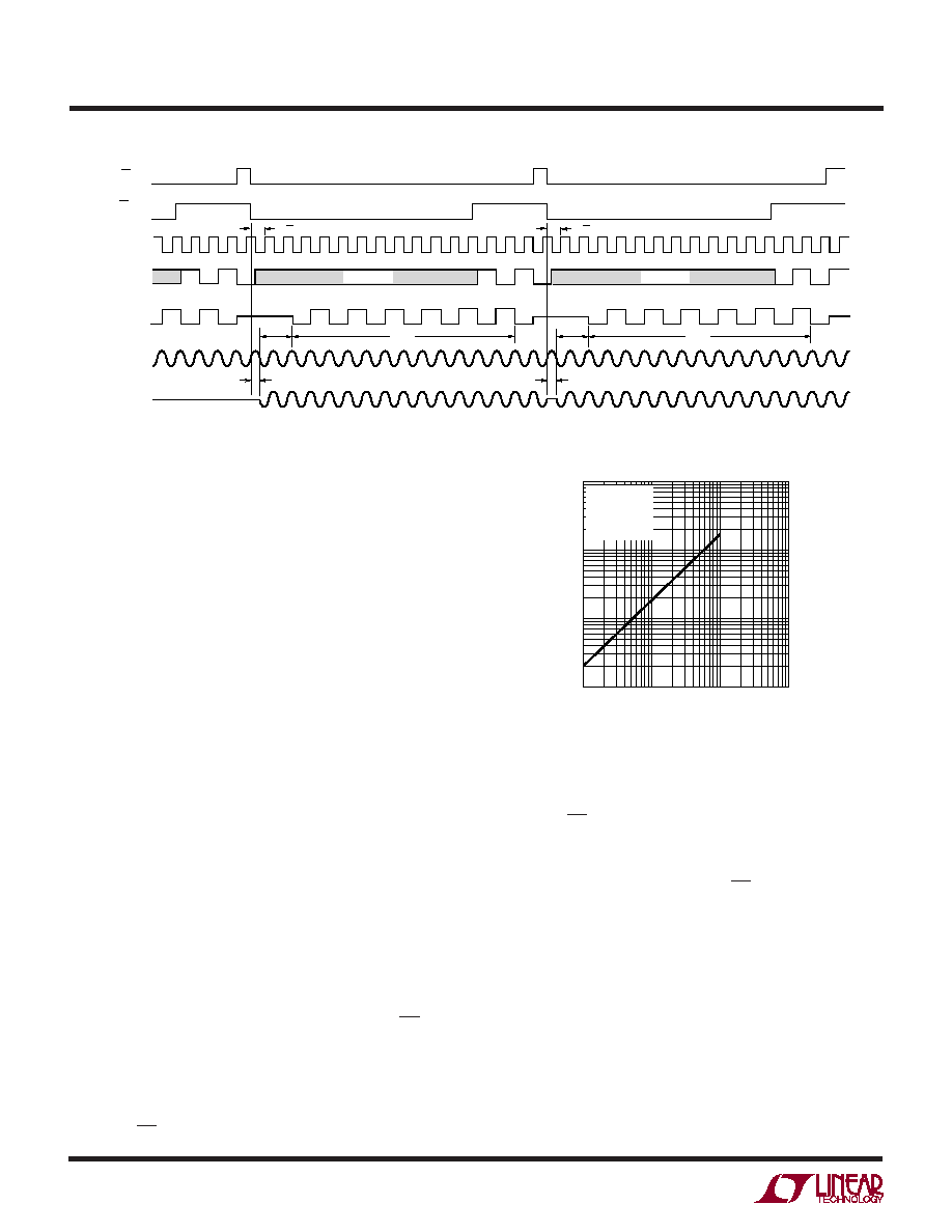
Figure 5. Use Separate Chip Selects to Maximize Sample Rate
Figure 6. Automatic Power Shutdown Between Conversions
Allows Power Consumption to Drop with Sample Rate
SAMPLE FREQUENCY (kHz)
0.1
1
SUPPLY
CURRENT
(
A)
10
100
1000
1
10
100
1594L/98L G01
TA = 25°C
VCC = 2.7V
VREF = 2.5V
fCLK = 200kHz
相关PDF资料 |
PDF描述 |
|---|---|
| MS3102R24-3S | CONN RCPT 7POS BOX MNT W/SCKT |
| LTC2444CUHF#PBF | IC ADC 24BIT HI SPEED 38QFN |
| MS3102A24-17S | CONN RCPT 5POS BOX MNT W/SCKT |
| VE-J4P-MW-F4 | CONVERTER MOD DC/DC 13.8V 100W |
| VE-J4L-MW-F2 | CONVERTER MOD DC/DC 28V 100W |
相关代理商/技术参数 |
参数描述 |
|---|---|
| LTC1595ACN8 | 功能描述:IC D/A CONV 16BIT MULTPLYNG 8DIP RoHS:否 类别:集成电路 (IC) >> 数据采集 - 数模转换器 系列:- 产品培训模块:Lead (SnPb) Finish for COTS Obsolescence Mitigation Program 标准包装:50 系列:- 设置时间:4µs 位数:12 数据接口:串行 转换器数目:2 电压电源:单电源 功率耗散(最大):- 工作温度:-40°C ~ 85°C 安装类型:表面贴装 封装/外壳:8-TSSOP,8-MSOP(0.118",3.00mm 宽) 供应商设备封装:8-uMAX 包装:管件 输出数目和类型:2 电压,单极 采样率(每秒):* 产品目录页面:1398 (CN2011-ZH PDF) |
| LTC1595ACN8#PBF | 功能描述:IC D/A CONV 16BIT MULTPLYNG 8DIP RoHS:是 类别:集成电路 (IC) >> 数据采集 - 数模转换器 系列:- 产品培训模块:Lead (SnPb) Finish for COTS Obsolescence Mitigation Program 标准包装:50 系列:- 设置时间:4µs 位数:12 数据接口:串行 转换器数目:2 电压电源:单电源 功率耗散(最大):- 工作温度:-40°C ~ 85°C 安装类型:表面贴装 封装/外壳:8-TSSOP,8-MSOP(0.118",3.00mm 宽) 供应商设备封装:8-uMAX 包装:管件 输出数目和类型:2 电压,单极 采样率(每秒):* 产品目录页面:1398 (CN2011-ZH PDF) |
| LTC1595ACS8 | 功能描述:IC D/A CONV 16BIT MULTPLYNG8SOIC RoHS:否 类别:集成电路 (IC) >> 数据采集 - 数模转换器 系列:- 产品培训模块:Data Converter Fundamentals DAC Architectures 标准包装:750 系列:- 设置时间:7µs 位数:16 数据接口:并联 转换器数目:1 电压电源:双 ± 功率耗散(最大):100mW 工作温度:0°C ~ 70°C 安装类型:表面贴装 封装/外壳:28-LCC(J 形引线) 供应商设备封装:28-PLCC(11.51x11.51) 包装:带卷 (TR) 输出数目和类型:1 电压,单极;1 电压,双极 采样率(每秒):143k |
| LTC1595ACS8#PBF | 功能描述:IC D/A CONV 16BIT MULTPLYNG8SOIC RoHS:是 类别:集成电路 (IC) >> 数据采集 - 数模转换器 系列:- 标准包装:1 系列:- 设置时间:4.5µs 位数:12 数据接口:串行,SPI? 转换器数目:1 电压电源:单电源 功率耗散(最大):- 工作温度:-40°C ~ 125°C 安装类型:表面贴装 封装/外壳:8-SOIC(0.154",3.90mm 宽) 供应商设备封装:8-SOICN 包装:剪切带 (CT) 输出数目和类型:1 电压,单极;1 电压,双极 采样率(每秒):* 其它名称:MCP4921T-E/SNCTMCP4921T-E/SNRCTMCP4921T-E/SNRCT-ND |
| LTC1595ACS8#TR | 功能描述:IC DAC 16BIT MULTIPLY SER 8SOIC RoHS:否 类别:集成电路 (IC) >> 数据采集 - 数模转换器 系列:- 产品培训模块:Data Converter Fundamentals DAC Architectures 标准包装:750 系列:- 设置时间:7µs 位数:16 数据接口:并联 转换器数目:1 电压电源:双 ± 功率耗散(最大):100mW 工作温度:0°C ~ 70°C 安装类型:表面贴装 封装/外壳:28-LCC(J 形引线) 供应商设备封装:28-PLCC(11.51x11.51) 包装:带卷 (TR) 输出数目和类型:1 电压,单极;1 电压,双极 采样率(每秒):143k |
发布紧急采购,3分钟左右您将得到回复。