- 您现在的位置:买卖IC网 > PDF目录8568 > LTC1596AISW#TR (Linear Technology)IC DAC 16BIT MULTIPLY SER 16SOIC PDF资料下载
参数资料
| 型号: | LTC1596AISW#TR |
| 厂商: | Linear Technology |
| 文件页数: | 14/16页 |
| 文件大小: | 0K |
| 描述: | IC DAC 16BIT MULTIPLY SER 16SOIC |
| 标准包装: | 1,000 |
| 设置时间: | 1µs |
| 位数: | 16 |
| 数据接口: | 串行 |
| 转换器数目: | 1 |
| 电压电源: | 单电源 |
| 功率耗散(最大): | 55µW |
| 工作温度: | -40°C ~ 85°C |
| 安装类型: | 表面贴装 |
| 封装/外壳: | 16-SOIC(0.295",7.50mm 宽) |
| 供应商设备封装: | 16-SOIC |
| 包装: | 带卷 (TR) |
| 输出数目和类型: | 1 电流,单极;1 电流,双极 |
| 采样率(每秒): | * |
LTC1595/LTC1596/LTC1596-1
7
159561fb
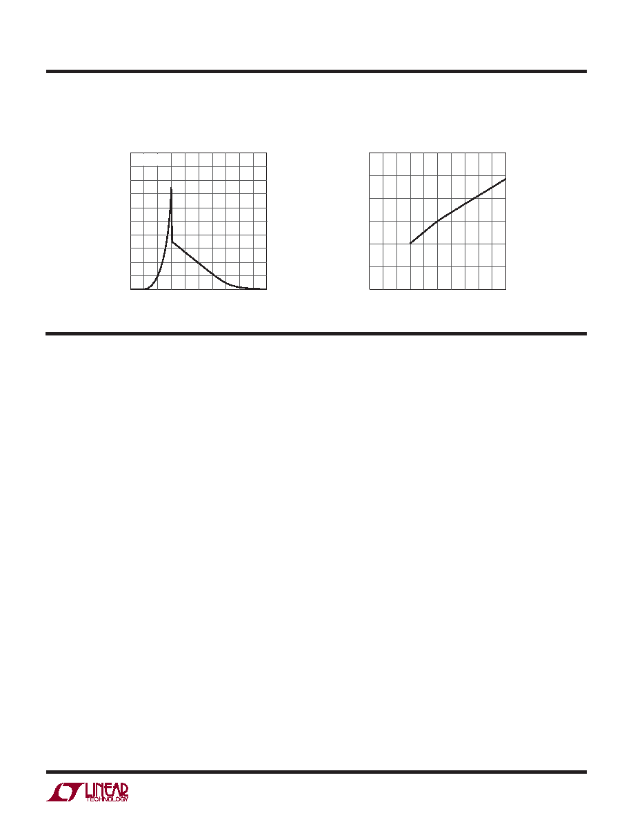
Typical perForMance characTerisTics
Supply Current
vs Logic Input Voltage
Logic Threshold
vs Supply Voltage
INPUT VOLTAGE (V)
0
SUPPLY
CURRENT
(mA)
0.6
0.8
1.0
4
1595/96 G10
0.4
0.2
0.5
0.7
0.9
0.3
0.1
0
1
2
3
5
VDD = 5V
SUPPLY VOLTAGE (V)
0
LOGIC
THRESHOLD
(V)
1.0
2.0
3.0
0.5
1.5
2.5
1595/96 G11
10
0
5
1
6
2
7
3
8
4
9
pin FuncTions
LTC1595
VREF (Pin 1): Reference Input.
RFB(Pin2):FeedbackResistor.Normallytiedtotheoutput
of the current to voltage converter op amp.
OUT1 (Pin 3): Current Output Pin. Tie to inverting input
of current to voltage converter op amp.
GND (Pin 4): Ground Pin.
LD (Pin 5): The Serial Interface Load Control Input. When
LD is pulled low, data is loaded from the shift register into
the DAC register, updating the DAC output.
SRI (Pin 6): The Serial Data Input. Data on the SRI pin
is latched into the shift register on the rising edge of the
serial clock. Data is loaded MSB first.
CLK (Pin 7): The Serial Interface Clock Input.
VDD (Pin 8): The Positive Supply Input. 4.5V ≤ VDD ≤ 5.5V.
Requires a bypass capacitor to ground.
LTC1596/LTC1596-1
OUT1 (Pin 1): True Current Output Pin. Tie to inverting
input of current to voltage converter op amp.
OUT2 (Pin 2): Complement Current Output Pin. Tie to
analog ground.
AGND (Pin 3): Analog Ground Pin.
STB1, STB2, STB3, STB4 (Pins 4, 8, 10, 11): Serial
Interface Clock Inputs. STB1, STB2 and STB4 are rising
edge triggered inputs. STB3 is a falling edge triggered
input (see Truth Tables).
LD1, LD2 (Pins 5, 9): Serial Interface Load Control Inputs.
When LD1 and LD2 are pulled low, data is loaded from
the shift register into the DAC register, updating the DAC
output (see Truth Tables).
SRO (Pin 6): The Output of the Shift Register. Becomes
valid on the active edge of the serial clock.
SRI (Pin 7): The Serial Data Input. Data on the SRI pin
is latched into the shift register on the active edge of the
serial clock. Data is loaded MSB first.
DGND (Pin 12): Digital Ground Pin.
CLR (Pin 13): The Clear Pin for the DAC. Clears DAC to
zero-scale when pulled low on LTC1596. Clears DAC to
mid-scale when pulled low on LTC1596-1. This pin should
be tied to VDD for normal operation.
VDD (Pin 14): The Positive Supply Input. 4.5V ≤ VDD ≤
5.5V. Requires a bypass capacitor to ground.
VREF (Pin 15): Reference Input.
RFB(Pin16):FeedbackResistor.Normallytiedtotheoutput
of the current to voltage converter op amp.
相关PDF资料 |
PDF描述 |
|---|---|
| LTC1596-1AISW#TRPBF | IC D/A CONV 16BIT MLTPLYNG16SOIC |
| LTC1596-1AISW#TR | IC DAC 16BIT MULTIPLY SER 16SOIC |
| AD7237AAN | IC DAC 12BIT W/AMP W/BUFF 24-DIP |
| VI-B6R-MY-B1 | CONVERTER MOD DC/DC 7.5V 50W |
| VI-27Z-MW-B1 | CONVERTER MOD DC/DC 2V 40W |
相关代理商/技术参数 |
参数描述 |
|---|---|
| LTC1596BCN | 功能描述:IC D/A CONV 16BIT MLTPLYNG 16DIP RoHS:否 类别:集成电路 (IC) >> 数据采集 - 数模转换器 系列:- 产品培训模块:Data Converter Fundamentals DAC Architectures 标准包装:750 系列:- 设置时间:7µs 位数:16 数据接口:并联 转换器数目:1 电压电源:双 ± 功率耗散(最大):100mW 工作温度:0°C ~ 70°C 安装类型:表面贴装 封装/外壳:28-LCC(J 形引线) 供应商设备封装:28-PLCC(11.51x11.51) 包装:带卷 (TR) 输出数目和类型:1 电压,单极;1 电压,双极 采样率(每秒):143k |
| LTC1596BCN#PBF | 制造商:Linear Technology 功能描述:DAC 1-CH R-2R 16-bit 16-Pin PDIP N |
| LTC1596BCSW | 功能描述:IC D/A CONV 16BIT MLTPLYNG16SOIC RoHS:否 类别:集成电路 (IC) >> 数据采集 - 数模转换器 系列:- 产品培训模块:Data Converter Fundamentals DAC Architectures 标准包装:750 系列:- 设置时间:7µs 位数:16 数据接口:并联 转换器数目:1 电压电源:双 ± 功率耗散(最大):100mW 工作温度:0°C ~ 70°C 安装类型:表面贴装 封装/外壳:28-LCC(J 形引线) 供应商设备封装:28-PLCC(11.51x11.51) 包装:带卷 (TR) 输出数目和类型:1 电压,单极;1 电压,双极 采样率(每秒):143k |
| LTC1596BCSW#PBF | 功能描述:IC D/A CONV 16BIT MLTPLYNG16SOIC RoHS:是 类别:集成电路 (IC) >> 数据采集 - 数模转换器 系列:- 产品培训模块:Lead (SnPb) Finish for COTS Obsolescence Mitigation Program 标准包装:50 系列:- 设置时间:4µs 位数:12 数据接口:串行 转换器数目:2 电压电源:单电源 功率耗散(最大):- 工作温度:-40°C ~ 85°C 安装类型:表面贴装 封装/外壳:8-TSSOP,8-MSOP(0.118",3.00mm 宽) 供应商设备封装:8-uMAX 包装:管件 输出数目和类型:2 电压,单极 采样率(每秒):* 产品目录页面:1398 (CN2011-ZH PDF) |
| LTC1596BCSW#TR | 功能描述:IC DAC 16BIT MULTIPLY SER 16SOIC RoHS:否 类别:集成电路 (IC) >> 数据采集 - 数模转换器 系列:- 产品培训模块:Data Converter Fundamentals DAC Architectures 标准包装:750 系列:- 设置时间:7µs 位数:16 数据接口:并联 转换器数目:1 电压电源:双 ± 功率耗散(最大):100mW 工作温度:0°C ~ 70°C 安装类型:表面贴装 封装/外壳:28-LCC(J 形引线) 供应商设备封装:28-PLCC(11.51x11.51) 包装:带卷 (TR) 输出数目和类型:1 电压,单极;1 电压,双极 采样率(每秒):143k |
发布紧急采购,3分钟左右您将得到回复。