- 您现在的位置:买卖IC网 > PDF目录8582 > LTC1597-1BIG#TRPBF (Linear Technology)IC D/A CONV 16BIT PAR 28-SSOP PDF资料下载
参数资料
| 型号: | LTC1597-1BIG#TRPBF |
| 厂商: | Linear Technology |
| 文件页数: | 5/20页 |
| 文件大小: | 0K |
| 描述: | IC D/A CONV 16BIT PAR 28-SSOP |
| 标准包装: | 2,000 |
| 设置时间: | 1µs |
| 位数: | 16 |
| 数据接口: | 并联 |
| 转换器数目: | 1 |
| 电压电源: | 单电源 |
| 功率耗散(最大): | 55µW |
| 工作温度: | -40°C ~ 85°C |
| 安装类型: | 表面贴装 |
| 封装/外壳: | 28-SSOP(0.209",5.30mm 宽) |
| 供应商设备封装: | 28-SSOP |
| 包装: | 带卷 (TR) |
| 输出数目和类型: | 1 电流,单极;1 电流,双极 |
| 采样率(每秒): | * |
13
LTC1591/LTC1597
15917fa
Description
The LTC1591/LTC1597 are 14-/16-bit multiplying, current
output DACs with a full parallel 14-/16-bit digital interface.
The devices operate from a single 5V supply and provide
both unipolar 0V to – 10V or 0V to 10V and bipolar
±10V
output ranges from a 10V or –10V reference input. They
have three additional precision resistors on chip for bipo-
lar operation. Refer to the block diagrams regarding the
following description.
The 14-/16-bit DACs consist of a precision R-2R ladder for
the 11/13LSBs. The 3MSBs are decoded into seven seg-
ments of resistor value R. Each of these segments and the
R-2R ladder carries an equally weighted current of one
eighth of full scale. The feedback resistor RFB and
4-quadrant resistor ROFS have a value of R/4. 4-quadrant
resistors R1 and R2 have a magnitude of R/4. R1 and R2
together with an external op amp (see Figure 2) inverts the
reference input voltage and applies it to the 14-/16-bit DAC
input REF, in 4-quadrant operation. The REF pin presents
a constant input impedance of R/8 in unipolar mode and
R/12 in bipolar mode. The output impedance of the current
output pin IOUT1 varies with DAC input code. The IOUT1
capacitance due to the NMOS current steering switches
also varies with input code from 70pF to 115pF. An added
feature of these devices, especially for waveform genera-
tion, is a proprietary deglitcher that reduces glitch energy
to below 2nV-s over the DAC output voltage range.
Digital Section
The LTC1591/LTC1597 are 14-/16-bit wide full parallel
data bus inputs. The devices are double-buffered with two
14-/16-bit registers. The double-buffered feature permits
the update of several DACs simultaneously. The input
register is loaded directly from a 16-bit microprocessor
bus when the WR pin is brought to a logic low level. The
second register (DAC register) is updated with the data
from the input register when the LD pin is brought to a
logic high level. Updating the DAC register updates the
DAC output with the new data. To make both registers
transparent for flowthrough mode, tie WR low and LD
high. However, this defeats the deglitcher operation and
output glitch impulse may increase. The deglitcher is
activated on the rising edge of the LD pin. The versatility
of the interface also allows the use of the input and DAC
registers in a master slave or edge-triggered configura-
tion. This mode of operation occurs when WR and LD are
tied together. The asynchronous clear pin resets the
LTC1591/LTC1597 to zero scale and the LTC1591-1/
LTC1597-1 to midscale. CLR resets both the input and
DAC registers. These devices also have a power-on reset.
Table 1 shows the truth table for the LTC1591/LT1597.
Unipolar Mode
(2-Quadrant Multiplying, VOUT = 0V to – VREF)
The LTC1591/LTC1597 can be used with a single op amp
to provide 2-quadrant multiplying operation as shown in
Figure 1. With a fixed – 10V reference, the circuits shown
give a precision unipolar 0V to 10V output swing.
APPLICATIONS INFORMATION
WU
U
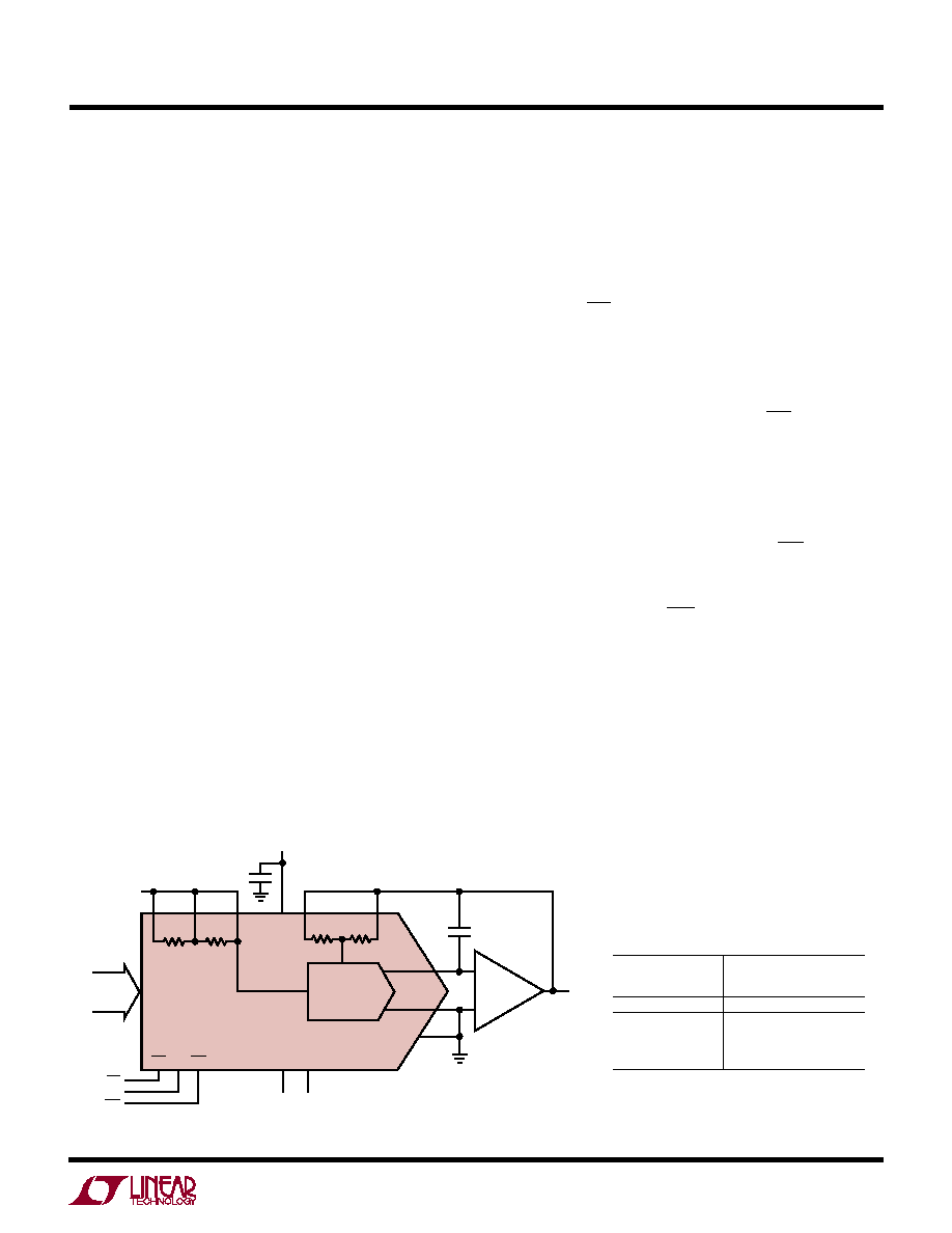
Figure 1a. Unipolar Operation (2-Quadrant Multiplication) VOUT = 0V to – VREF
VCC
LTC1591
RFB
ROFS
5V
LD
3
2
98
28
27
23
7
22
R1
RCOM
1
REF
4
5
0.1
μF
6
IOUT1
33pF
VOUT =
0V TO
–VREF
1591/97 F01a
AGND
DGND
WR
10 TO 21,
24, 25
WR
CLR
NC
CLR
VREF
–
+
LT1001
14-BIT DAC
R1
R2
14
DATA
INPUTS
Unipolar Binary Code Table
DIGITAL INPUT
BINARY NUMBER
IN DAC REGISTER
–VREF (16,383/16,384)
–VREF (8,192/16,384) = –VREF/2
–VREF (1/16,384)
0V
LSB
1111 1111
11
0000 0000
00
0000 0000
01
0000 0000
00
ANALOG OUTPUT
VOUT
MSB
1111
1000
0000
26
NC
相关PDF资料 |
PDF描述 |
|---|---|
| LTC2755BCUP-16#TRPBF | IC DAC 16BIT CUR OUT 64-QFN |
| AD7840KNZ | IC DAC 14BIT LC2MOS VOUT 24-DIP |
| AD7248AAP | IC DAC 12BIT W/REF 28-PLCC |
| AD5570WRSZ-REEL | IC DAC 16BIT SERIAL IN 16SSOP |
| AD5544ARSZ-REEL7 | IC DAC 16BIT QUAD SRL 28SSOP |
相关代理商/技术参数 |
参数描述 |
|---|---|
| LTC1597-1BIN | 功能描述:IC D/A CONV 16BIT PAR 28-DIP RoHS:否 类别:集成电路 (IC) >> 数据采集 - 数模转换器 系列:- 产品培训模块:Data Converter Fundamentals DAC Architectures 标准包装:750 系列:- 设置时间:7µs 位数:16 数据接口:并联 转换器数目:1 电压电源:双 ± 功率耗散(最大):100mW 工作温度:0°C ~ 70°C 安装类型:表面贴装 封装/外壳:28-LCC(J 形引线) 供应商设备封装:28-PLCC(11.51x11.51) 包装:带卷 (TR) 输出数目和类型:1 电压,单极;1 电压,双极 采样率(每秒):143k |
| LTC1597-1BIN#PBF | 功能描述:IC CONV D/A 16BIT PAR 28-DIP RoHS:是 类别:集成电路 (IC) >> 数据采集 - 数模转换器 系列:- 标准包装:2,400 系列:- 设置时间:- 位数:18 数据接口:串行 转换器数目:3 电压电源:模拟和数字 功率耗散(最大):- 工作温度:-40°C ~ 85°C 安装类型:表面贴装 封装/外壳:36-TFBGA 供应商设备封装:36-TFBGA 包装:带卷 (TR) 输出数目和类型:* 采样率(每秒):* |
| LTC1597ACG | 功能描述:IC D/A CONV 16BIT PAR 28-SSOP RoHS:否 类别:集成电路 (IC) >> 数据采集 - 数模转换器 系列:- 产品培训模块:Data Converter Fundamentals DAC Architectures 标准包装:750 系列:- 设置时间:7µs 位数:16 数据接口:并联 转换器数目:1 电压电源:双 ± 功率耗散(最大):100mW 工作温度:0°C ~ 70°C 安装类型:表面贴装 封装/外壳:28-LCC(J 形引线) 供应商设备封装:28-PLCC(11.51x11.51) 包装:带卷 (TR) 输出数目和类型:1 电压,单极;1 电压,双极 采样率(每秒):143k |
| LTC1597ACG#PBF | 功能描述:IC D/A CONV 16BIT PAR 28-SSOP RoHS:是 类别:集成电路 (IC) >> 数据采集 - 数模转换器 系列:- 标准包装:1 系列:- 设置时间:4.5µs 位数:12 数据接口:串行,SPI? 转换器数目:1 电压电源:单电源 功率耗散(最大):- 工作温度:-40°C ~ 125°C 安装类型:表面贴装 封装/外壳:8-SOIC(0.154",3.90mm 宽) 供应商设备封装:8-SOICN 包装:剪切带 (CT) 输出数目和类型:1 电压,单极;1 电压,双极 采样率(每秒):* 其它名称:MCP4921T-E/SNCTMCP4921T-E/SNRCTMCP4921T-E/SNRCT-ND |
| LTC1597ACG#PBF | 制造商:Linear Technology 功能描述:DAC, 16BIT, SSOP-28 |
发布紧急采购,3分钟左右您将得到回复。