参数资料
| 型号: | LTC1597-1BIG |
| 厂商: | Linear Technology |
| 文件页数: | 6/20页 |
| 文件大小: | 0K |
| 描述: | IC D/A CONV 16BIT PAR 28-SSOP |
| 标准包装: | 47 |
| 设置时间: | 1µs |
| 位数: | 16 |
| 数据接口: | 并联 |
| 转换器数目: | 1 |
| 电压电源: | 单电源 |
| 功率耗散(最大): | 55µW |
| 工作温度: | -40°C ~ 85°C |
| 安装类型: | 表面贴装 |
| 封装/外壳: | 28-SSOP(0.209",5.30mm 宽) |
| 供应商设备封装: | 28-SSOP |
| 包装: | 管件 |
| 输出数目和类型: | 1 电流,单极;1 电流,双极 |
| 采样率(每秒): | * |
14
LTC1591/LTC1597
15917fa
APPLICATIONS INFORMATION
WU
U
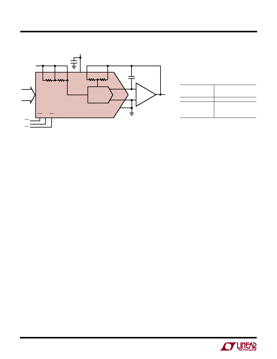
Figure 1b. Unipolar Operation (2-Quadrant Multiplication) VOUT = 0V to – VREF
Bipolar Mode
(4-Quadrant Multiplying, VOUT = – VREF to VREF)
The LTC1591/LTC1597 contain on chip all the 4-quadrant
resistors necessary for bipolar operation. 4-quadrant
multiplying operation can be achieved with a minimum of
external components, a capacitor and a dual op amp, as
shown in Figure 2. With a fixed 10V reference, the circuit
shown gives a precision bipolar – 10V to 10V output
swing.
Op Amp Selection
Because of the extremely high accuracy of the 14-/16-bit
LTC1591/LTC1597, thought should be given to op amp
selection in order to achieve the exceptional performance
of which the part is capable. Fortunately, the sensitivity of
INL and DNL to op amp offset has been greatly reduced
compared to previous generations of multiplying DACs.
Op amp offset will contribute mostly to output offset and
gain and will have minimal effect on INL and DNL. For the
LTC1597, a 500
μVopampoffsetwillcauseabout0.55LSB
INL degradation and 0.15LSB DNL degradation with a 10V
full-scale range. The main effects of op amp offset will be
a degradation of zero-scale error equal to the op amp
offset, and a degradation of full-scale error equal to twice
the op amp offset. For the LTC1597, the same 500
μV op
amp offset (2mV offset for LTC1591) will cause a 3.3LSB
zero-scale error and a 6.5LSB full-scale error with a 10V
full-scale range.
Op amp input bias current (IBIAS) contributes only a zero-
scale error equal to IBIAS(RFB/ROFS) = IBIAS(6k). For a
thorough discussion of 16-bit DAC settling time and op
amp selection, refer to Application Note 74, “
Component
and Measurement Advances Ensure 16-Bit DAC Settling
Time.”
Reference Input and Grounding
For optimum performance the reference input of the
LTC1597 should be driven by a source impedance of less
than 1k
Ω. However, these DACs have been designed to
minimize source impedance effects. An 8k
Ω source im-
pedance degrades both INL and DNL by 0.2LSB.
As with any high resolution converter, clean grounding is
important. A low impedance analog ground plane and star
grounding should be used. AGND must be tied to the star
ground with as low a resistance as possible.
VCC
LTC1597
RFB
ROFS
5V
LD
3
2
98
28
23
7
22
R1
RCOM
1
REF
4
5
0.1
μF
6
IOUT1
33pF
VOUT =
0V TO
–VREF
1591/97 F01b
AGND
DGND
WR
10 TO 21,
24 TO 27
WR
CLR
VREF
–
+
LT1001
16-BIT DAC
R1
R2
16
DATA
INPUTS
Unipolar Binary Code Table
DIGITAL INPUT
BINARY NUMBER
IN DAC REGISTER
–VREF (65,535/65,536)
–VREF (32,768/65,536) = –VREF/2
–VREF (1/65,536)
0V
LSB
1111 1111
1111
0000 0000
0000
0000 0000
0001
0000 0000
0000
ANALOG OUTPUT
VOUT
MSB
1111
1000
0000
相关PDF资料 |
PDF描述 |
|---|---|
| LTC1597-1BIG#TRPBF | IC D/A CONV 16BIT PAR 28-SSOP |
| LTC2755BCUP-16#TRPBF | IC DAC 16BIT CUR OUT 64-QFN |
| AD7840KNZ | IC DAC 14BIT LC2MOS VOUT 24-DIP |
| AD7248AAP | IC DAC 12BIT W/REF 28-PLCC |
| AD5570WRSZ-REEL | IC DAC 16BIT SERIAL IN 16SSOP |
相关代理商/技术参数 |
参数描述 |
|---|---|
| LTC1597-1BIG#PBF | 功能描述:IC D/A CONV 16BIT PAR 28-SSOP RoHS:是 类别:集成电路 (IC) >> 数据采集 - 数模转换器 系列:- 产品培训模块:Data Converter Fundamentals DAC Architectures 标准包装:750 系列:- 设置时间:7µs 位数:16 数据接口:并联 转换器数目:1 电压电源:双 ± 功率耗散(最大):100mW 工作温度:0°C ~ 70°C 安装类型:表面贴装 封装/外壳:28-LCC(J 形引线) 供应商设备封装:28-PLCC(11.51x11.51) 包装:带卷 (TR) 输出数目和类型:1 电压,单极;1 电压,双极 采样率(每秒):143k |
| LTC1597-1BIG#TR | 功能描述:IC DAC 16BIT PAR 28SSOP RoHS:否 类别:集成电路 (IC) >> 数据采集 - 数模转换器 系列:- 产品培训模块:Data Converter Fundamentals DAC Architectures 标准包装:750 系列:- 设置时间:7µs 位数:16 数据接口:并联 转换器数目:1 电压电源:双 ± 功率耗散(最大):100mW 工作温度:0°C ~ 70°C 安装类型:表面贴装 封装/外壳:28-LCC(J 形引线) 供应商设备封装:28-PLCC(11.51x11.51) 包装:带卷 (TR) 输出数目和类型:1 电压,单极;1 电压,双极 采样率(每秒):143k |
| LTC1597-1BIG#TRPBF | 功能描述:IC D/A CONV 16BIT PAR 28-SSOP RoHS:是 类别:集成电路 (IC) >> 数据采集 - 数模转换器 系列:- 产品培训模块:Data Converter Fundamentals DAC Architectures 标准包装:750 系列:- 设置时间:7µs 位数:16 数据接口:并联 转换器数目:1 电压电源:双 ± 功率耗散(最大):100mW 工作温度:0°C ~ 70°C 安装类型:表面贴装 封装/外壳:28-LCC(J 形引线) 供应商设备封装:28-PLCC(11.51x11.51) 包装:带卷 (TR) 输出数目和类型:1 电压,单极;1 电压,双极 采样率(每秒):143k |
| LTC1597-1BIN | 功能描述:IC D/A CONV 16BIT PAR 28-DIP RoHS:否 类别:集成电路 (IC) >> 数据采集 - 数模转换器 系列:- 产品培训模块:Data Converter Fundamentals DAC Architectures 标准包装:750 系列:- 设置时间:7µs 位数:16 数据接口:并联 转换器数目:1 电压电源:双 ± 功率耗散(最大):100mW 工作温度:0°C ~ 70°C 安装类型:表面贴装 封装/外壳:28-LCC(J 形引线) 供应商设备封装:28-PLCC(11.51x11.51) 包装:带卷 (TR) 输出数目和类型:1 电压,单极;1 电压,双极 采样率(每秒):143k |
| LTC1597-1BIN#PBF | 功能描述:IC CONV D/A 16BIT PAR 28-DIP RoHS:是 类别:集成电路 (IC) >> 数据采集 - 数模转换器 系列:- 标准包装:2,400 系列:- 设置时间:- 位数:18 数据接口:串行 转换器数目:3 电压电源:模拟和数字 功率耗散(最大):- 工作温度:-40°C ~ 85°C 安装类型:表面贴装 封装/外壳:36-TFBGA 供应商设备封装:36-TFBGA 包装:带卷 (TR) 输出数目和类型:* 采样率(每秒):* |
发布紧急采购,3分钟左右您将得到回复。