参数资料
| 型号: | LTC1598LCG |
| 厂商: | Linear Technology |
| 文件页数: | 9/24页 |
| 文件大小: | 0K |
| 描述: | IC A/D CONV 12BIT SRL 8CH 24SSOP |
| 标准包装: | 59 |
| 位数: | 12 |
| 采样率(每秒): | 10.5k |
| 数据接口: | MICROWIRE?,QSPI?,串行,SPI? |
| 转换器数目: | 1 |
| 功率耗散(最大): | 480µW |
| 电压电源: | 单电源 |
| 工作温度: | 0°C ~ 70°C |
| 安装类型: | 表面贴装 |
| 封装/外壳: | 24-SSOP(0.209",5.30mm 宽) |
| 供应商设备封装: | 24-SSOP |
| 包装: | 管件 |
| 输入数目和类型: | 8 个单端,单极 |
17
LTC1594L/LTC1598L
15948lfb
Input Leakage Current
Input leakage currents can also create errors if the source
resistance gets too large. For instance, the maximum
input leakage specification of 200nA (at 85
°C) flowing
through a source resistance of 600
will cause a voltage
drop of 120
V or 0.2LSB. This error will be much
reduced at lower temperatures because leakage drops
rapidly (see typical curve Input Channel Leakage Current
vs Temperature).
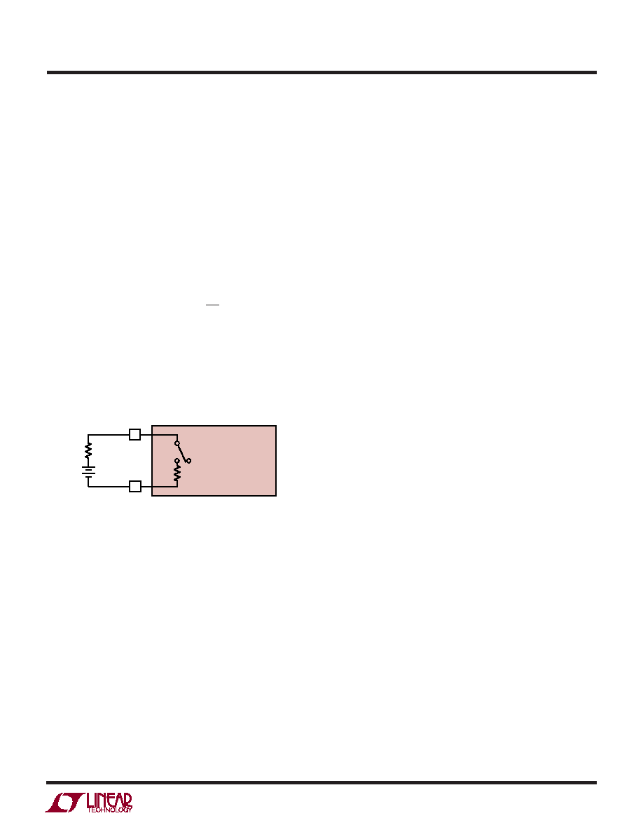
REFERENCE INPUTS
The reference input of the LTC1594L/LTC1598L is effec-
tively a 50k resistor from the time CS goes low to the end
of the conversion. The reference input becomes a high
impedance node at any other time (see Figure 9). Since
the voltage on the reference input defines the voltage
span of the A/D converter, the reference input should be
driven by a reference with low ROUT (ex. LT1004, LT1019
and LT1021) or a voltage source with low ROUT.
Reduced Reference Operation
The effective resolution of the LTC1594L/LTC1598L can
be increased by reducing the input span of the convert-
ers. The LTC1594L/LTC1598L exhibit good linearity and
gain over a wide range of reference voltages (see typical
curves Change in Linearity vs Reference Voltage and
Change in Gain vs Reference Voltage). However, care
must be taken when operating at low values of VREF
because of the reduced LSB step size and the resulting
higher accuracy requirement placed on the converters.
The following factors must be considered when operat-
ing at low VREF values:
1. Offset
2. Noise
3. Conversion speed (CLK frequency)
Offset with Reduced VREF
The offset of the LTC1594L/LTC1598L has a larger effect
on the output code when the ADCs are operated with
reduced reference voltage. The offset (which is typically
a fixed voltage) becomes a larger fraction of an LSB as the
size of the LSB is reduced. The typical curve of Change in
Offset vs Reference Voltage shows how offset in LSBs is
related to reference voltage for a typical value of VOS. For
example, a VOS of 122V which is 0.2LSB with a 2.5V
reference becomes 0.5LSB with a 1V reference and
2.5LSBs with a 0.2V reference. If this offset is unaccept-
able, it can be corrected digitally by the receiving system
or by offsetting the “COM” input of the LTC1594L/
LTC1598L.
Noise with Reduced VREF
The total input referred noise of the LTC1594L/LTC1598L
can be reduced to approximately 400
V peak-to-peak
using a ground plane, good bypassing, good layout
techniques and minimizing noise on the reference inputs.
This noise is insignificant with a 5V reference but will
become a larger fraction of an LSB as the size of the LSB
is reduced.
For operation with a 2.5V reference, the 400
V noise is
only 0.66LSB peak-to-peak. In this case, the LTC1594L/
LTC1598L noise will contribute virtually no uncertainty to
the output code. However, for reduced references the
noise may become a significant fraction of an LSB and
cause undesirable jitter in the output code. For example,
with a 1.25V reference this same 400
V noise is 1.32LSB
peak-to-peak. This will reduce the range of input voltages
over which a stable output code can be achieved by 1LSB.
If the reference is further reduced to 1V, the 400
V noise
becomes equal to 1.65LSBs and a stable code may be
difficult to achieve. In this case, averaging multiple
readings may be necessary.
This noise data was taken in a very clean setup. Any setup
induced noise (noise or ripple on VCC, VREF or VIN) will
add to the internal noise. The lower the reference voltage
to be used the more critical it becomes to have a clean,
noise free setup.
LTC1594L
LTC1598L
REF+
ROUT
VREF
1
4
GND
1594L/98L F09
Figure 9. Reference Input Equivalent Circuit
APPLICATIONS INFORMATION
WU
U
相关PDF资料 |
PDF描述 |
|---|---|
| LTC1599AIG#TRPBF | IC D/A CONV 16BIT MLTPLYNG24SSOP |
| LTC1603IG#TRPBF | IC ADC W/SHUTDOWN 16BIT 36-SSOP |
| LTC1604AIG#TR | IC ADC 16BIT SAMPL SHTDWN 36SSOP |
| LTC1605-1IN#PBF | IC A/D CONV 16BIT SAMPLNG 28-DIP |
| LTC1605AISW#TR | IC ADC 16BIT 5V SAMPLING 28SOIC |
相关代理商/技术参数 |
参数描述 |
|---|---|
| LTC1598LCG#PBF | 功能描述:IC A/D CONV 12BIT SRL 8CH 24SSOP RoHS:是 类别:集成电路 (IC) >> 数据采集 - 模数转换器 系列:- 标准包装:1 系列:microPOWER™ 位数:8 采样率(每秒):1M 数据接口:串行,SPI? 转换器数目:1 功率耗散(最大):- 电压电源:模拟和数字 工作温度:-40°C ~ 125°C 安装类型:表面贴装 封装/外壳:24-VFQFN 裸露焊盘 供应商设备封装:24-VQFN 裸露焊盘(4x4) 包装:Digi-Reel® 输入数目和类型:8 个单端,单极 产品目录页面:892 (CN2011-ZH PDF) 其它名称:296-25851-6 |
| LTC1598LCG#TR | 功能描述:IC ADC 12BIT 3V 8CH SAMPL 24SSOP RoHS:否 类别:集成电路 (IC) >> 数据采集 - 模数转换器 系列:- 标准包装:1,000 系列:- 位数:16 采样率(每秒):45k 数据接口:串行 转换器数目:2 功率耗散(最大):315mW 电压电源:模拟和数字 工作温度:0°C ~ 70°C 安装类型:表面贴装 封装/外壳:28-SOIC(0.295",7.50mm 宽) 供应商设备封装:28-SOIC W 包装:带卷 (TR) 输入数目和类型:2 个单端,单极 |
| LTC1598LCG#TRPBF | 功能描述:IC A/D CONV 12BIT SRL 8CH 24SSOP RoHS:是 类别:集成电路 (IC) >> 数据采集 - 模数转换器 系列:- 标准包装:1,000 系列:- 位数:16 采样率(每秒):45k 数据接口:串行 转换器数目:2 功率耗散(最大):315mW 电压电源:模拟和数字 工作温度:0°C ~ 70°C 安装类型:表面贴装 封装/外壳:28-SOIC(0.295",7.50mm 宽) 供应商设备封装:28-SOIC W 包装:带卷 (TR) 输入数目和类型:2 个单端,单极 |
| LTC1598LIG | 功能描述:IC A/D CONV 12BIT SRL 8CH 24SSOP RoHS:否 类别:集成电路 (IC) >> 数据采集 - 模数转换器 系列:- 标准包装:1,000 系列:- 位数:16 采样率(每秒):45k 数据接口:串行 转换器数目:2 功率耗散(最大):315mW 电压电源:模拟和数字 工作温度:0°C ~ 70°C 安装类型:表面贴装 封装/外壳:28-SOIC(0.295",7.50mm 宽) 供应商设备封装:28-SOIC W 包装:带卷 (TR) 输入数目和类型:2 个单端,单极 |
| LTC1598LIG#PBF | 功能描述:IC A/D CONV 12BIT SRL 8CH 24SSOP RoHS:是 类别:集成电路 (IC) >> 数据采集 - 模数转换器 系列:- 标准包装:1,000 系列:- 位数:16 采样率(每秒):45k 数据接口:串行 转换器数目:2 功率耗散(最大):315mW 电压电源:模拟和数字 工作温度:0°C ~ 70°C 安装类型:表面贴装 封装/外壳:28-SOIC(0.295",7.50mm 宽) 供应商设备封装:28-SOIC W 包装:带卷 (TR) 输入数目和类型:2 个单端,单极 |
发布紧急采购,3分钟左右您将得到回复。