- 您现在的位置:买卖IC网 > PDF目录10278 > LTC1598LIG#PBF (Linear Technology)IC A/D CONV 12BIT SRL 8CH 24SSOP PDF资料下载
参数资料
| 型号: | LTC1598LIG#PBF |
| 厂商: | Linear Technology |
| 文件页数: | 8/24页 |
| 文件大小: | 0K |
| 描述: | IC A/D CONV 12BIT SRL 8CH 24SSOP |
| 标准包装: | 59 |
| 位数: | 12 |
| 采样率(每秒): | 10.5k |
| 数据接口: | MICROWIRE?,QSPI?,串行,SPI? |
| 转换器数目: | 1 |
| 功率耗散(最大): | 480µW |
| 电压电源: | 单电源 |
| 工作温度: | -40°C ~ 85°C |
| 安装类型: | 表面贴装 |
| 封装/外壳: | 24-SSOP(0.209",5.30mm 宽) |
| 供应商设备封装: | 24-SSOP |
| 包装: | 管件 |
| 输入数目和类型: | 8 个单端,单极 |
16
LTC1594L/LTC1598L
15948lfb
APPLICATIONS INFORMATION
WU
U
edge, the S & H goes into hold mode and the conversion
begins. The voltage on the “COM” input must remain
constant and be free of noise and ripple throughout the
conversion time. Otherwise, the conversion operation
may not be performed accurately. The conversion time is
12 CLK cycles. Therefore, a change in the “COM” input
voltage during this interval can cause conversion errors.
For a sinusoidal voltage on the “COM” input this error
would be:
VERROR(MAX) = VPEAK(2π)(f)(“COM”)12/fCLK
Where f(“COM”) is the frequency of the “COM” input
voltage, VPEAK is its peak amplitude and fCLK is the
frequency of the CLK. In most cases, VERROR will not be
significant. For a 60Hz signal on the “COM” input to
generate a 0.5LSB error (305
V) with the converter
running at CLK = 200kHz, its peak value would have to be
5.266mV.
ANALOG INPUTS
Because of the capacitive redistribution A/D conversion
techniques used, the analog inputs of the LTC1594L/
LTC1598L have capacitive switching input current spikes.
These current spikes settle quickly and do not cause a
problem. However, if large source resistances are used
or if slow settling op amps drive the inputs, care must be
taken to insure that the transients caused by the current
spikes settle completely before the conversion begins.
“Analog” Input Settling
The input capacitor of the LTC1594L/LTC1598L is switched
onto the selected channel input during the tSMPL time (see
Figure 7) and samples the input signal within that time. The
sample phase is at least 1 1/2 CLK cycles before conver-
sion starts. The voltage on the “analog” input must settle
completely within tSMPL. Minimizing RSOURCE+ and C1 will
improve the input settling time. If a large “analog” input
source resistance must be used, the sample time can be
increased by using a slower CLK frequency.
“COM” Input Settling
At the end of the tSMPL, the input capacitor switches to the
“COM” input and conversion starts (see Figures 1 and 7).
During the conversion, the “analog” input voltage is
effectively “held” by the sample-and-hold and will not
affect the conversion result. However, it is critical that the
“COM” input voltage settles completely during the first
CLK cycle of the conversion time and be free of noise.
Minimizing RSOURCE– and C2 will improve settling time.
If a large “COM” input source resistance must be used,
the time allowed for settling can be extended by using a
slower CLK frequency.
Input Op Amps
When driving the analog inputs with an op amp it is
important that the op amp settle within the allowed time
(see Figure 7). Again, the “analog” and “COM” input
sampling times can be extended as described above to
accommodate slower op amps. Most op amps, including
the LT
1006 and LT1413 single supply op amps, can be
made to settle well even with the minimum settling
windows of 7.5
s (“analog” input) which occur at the
maximum clock rate of 200kHz.
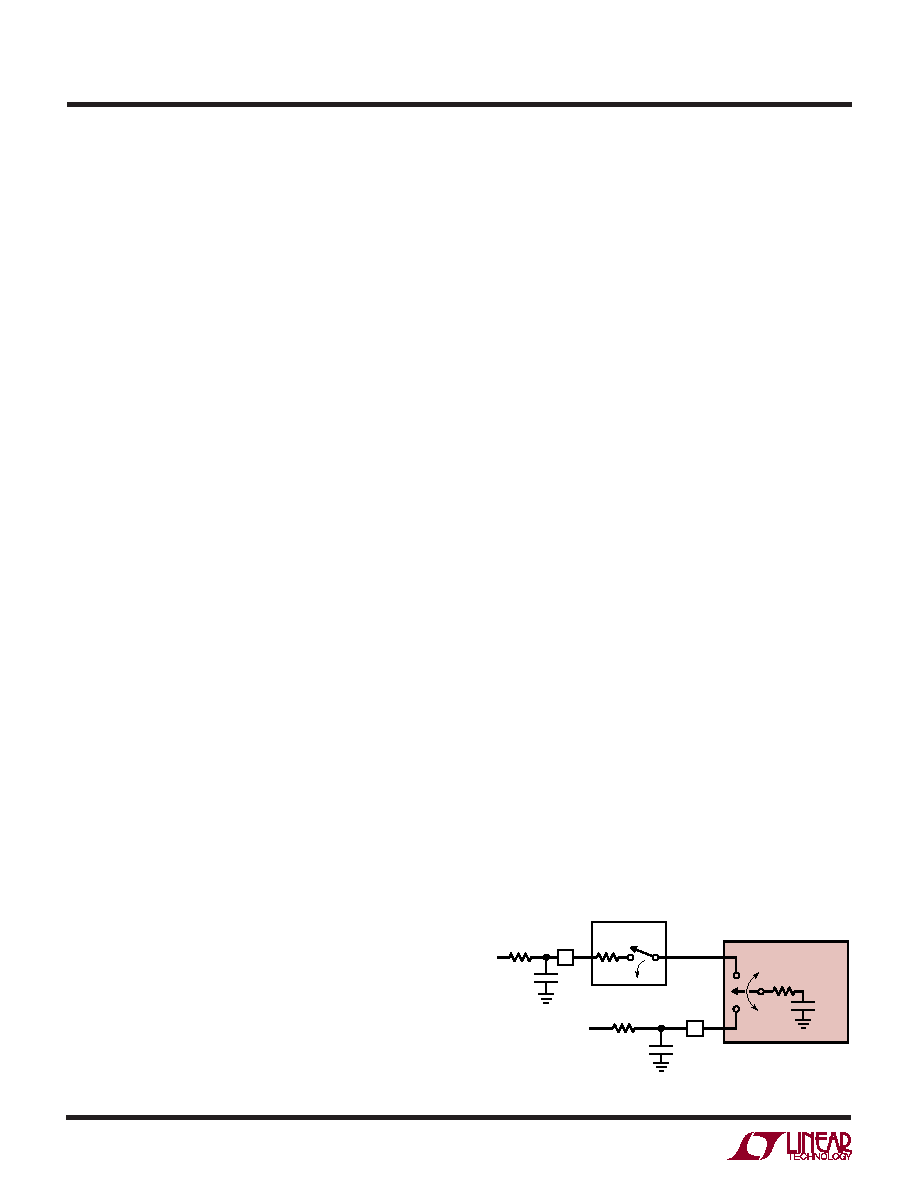
Source Resistance
The analog inputs of the LTC1594L/LTC1598L look like a
20pF capacitor (CIN) in series with a 1k resistor (RON) and
a 90
channel resistance as shown in Figure 8. CIN gets
switched between the selected “analog” and “COM”
inputs once during each conversion cycle. Large external
source resistors and capacitances will slow the settling
of the inputs. It is important that the overall RC time
constants be short enough to allow the analog inputs to
completely settle within the allowed time.
Figure 8. Analog Input Equivalent Circuit
RON
1k
RON
90
CIN
20pF
LTC1594L
LTC1598L
“ANALOG”
INPUT
RSOURCE+
VIN+
C1
“COM”
INPUT
MUXOUT
MUX
ADCIN
RSOURCE–
VIN–
C2
1594L/98L F08
相关PDF资料 |
PDF描述 |
|---|---|
| MS27497T24B4BA | CONN HSG RCPT 56POS WALL MT SCKT |
| VE-JNR-MX-S | CONVERTER MOD DC/DC 7.5V 75W |
| VE-JNP-MX-S | CONVERTER MOD DC/DC 13.8V 75W |
| D38999/26WG75SNLC | CONN HSG PLUG 4POS STRGHT SCKT |
| LTC1598LIG | IC A/D CONV 12BIT SRL 8CH 24SSOP |
相关代理商/技术参数 |
参数描述 |
|---|---|
| LTC1599ACG | 功能描述:IC D/A CONV 16BIT MLTPLYNG24SSOP RoHS:否 类别:集成电路 (IC) >> 数据采集 - 数模转换器 系列:- 产品培训模块:Data Converter Fundamentals DAC Architectures 标准包装:750 系列:- 设置时间:7µs 位数:16 数据接口:并联 转换器数目:1 电压电源:双 ± 功率耗散(最大):100mW 工作温度:0°C ~ 70°C 安装类型:表面贴装 封装/外壳:28-LCC(J 形引线) 供应商设备封装:28-PLCC(11.51x11.51) 包装:带卷 (TR) 输出数目和类型:1 电压,单极;1 电压,双极 采样率(每秒):143k |
| LTC1599ACG#PBF | 功能描述:IC D/A CONV 16BIT MLTPLYNG24SSOP RoHS:是 类别:集成电路 (IC) >> 数据采集 - 数模转换器 系列:- 产品培训模块:Data Converter Fundamentals DAC Architectures 标准包装:750 系列:- 设置时间:7µs 位数:16 数据接口:并联 转换器数目:1 电压电源:双 ± 功率耗散(最大):100mW 工作温度:0°C ~ 70°C 安装类型:表面贴装 封装/外壳:28-LCC(J 形引线) 供应商设备封装:28-PLCC(11.51x11.51) 包装:带卷 (TR) 输出数目和类型:1 电压,单极;1 电压,双极 采样率(每秒):143k |
| LTC1599ACG#TR | 功能描述:IC DAC 16BIT PARALLEL IN 24SSOP RoHS:否 类别:集成电路 (IC) >> 数据采集 - 数模转换器 系列:- 产品培训模块:Data Converter Fundamentals DAC Architectures 标准包装:750 系列:- 设置时间:7µs 位数:16 数据接口:并联 转换器数目:1 电压电源:双 ± 功率耗散(最大):100mW 工作温度:0°C ~ 70°C 安装类型:表面贴装 封装/外壳:28-LCC(J 形引线) 供应商设备封装:28-PLCC(11.51x11.51) 包装:带卷 (TR) 输出数目和类型:1 电压,单极;1 电压,双极 采样率(每秒):143k |
| LTC1599ACG#TRPBF | 功能描述:IC D/A CONV 16BIT MLTPLYNG24SSOP RoHS:是 类别:集成电路 (IC) >> 数据采集 - 数模转换器 系列:- 产品培训模块:Data Converter Fundamentals DAC Architectures 标准包装:750 系列:- 设置时间:7µs 位数:16 数据接口:并联 转换器数目:1 电压电源:双 ± 功率耗散(最大):100mW 工作温度:0°C ~ 70°C 安装类型:表面贴装 封装/外壳:28-LCC(J 形引线) 供应商设备封装:28-PLCC(11.51x11.51) 包装:带卷 (TR) 输出数目和类型:1 电压,单极;1 电压,双极 采样率(每秒):143k |
| LTC1599ACN | 功能描述:IC DAC 16BIT PARALLEL IN 24DIP RoHS:否 类别:集成电路 (IC) >> 数据采集 - 数模转换器 系列:- 产品培训模块:Data Converter Fundamentals DAC Architectures 标准包装:750 系列:- 设置时间:7µs 位数:16 数据接口:并联 转换器数目:1 电压电源:双 ± 功率耗散(最大):100mW 工作温度:0°C ~ 70°C 安装类型:表面贴装 封装/外壳:28-LCC(J 形引线) 供应商设备封装:28-PLCC(11.51x11.51) 包装:带卷 (TR) 输出数目和类型:1 电压,单极;1 电压,双极 采样率(每秒):143k |
发布紧急采购,3分钟左右您将得到回复。