- 您现在的位置:买卖IC网 > PDF目录8565 > LTC1599AIG#PBF (Linear Technology)IC D/A CONV 16BIT MLTPLYNG24SSOP PDF资料下载
参数资料
| 型号: | LTC1599AIG#PBF |
| 厂商: | Linear Technology |
| 文件页数: | 5/20页 |
| 文件大小: | 0K |
| 描述: | IC D/A CONV 16BIT MLTPLYNG24SSOP |
| 标准包装: | 59 |
| 设置时间: | 1µs |
| 位数: | 16 |
| 数据接口: | 并联 |
| 转换器数目: | 1 |
| 电压电源: | 单电源 |
| 功率耗散(最大): | 55µW |
| 工作温度: | -40°C ~ 85°C |
| 安装类型: | 表面贴装 |
| 封装/外壳: | 24-SSOP(0.209",5.30mm 宽) |
| 供应商设备封装: | 24-SSOP |
| 包装: | 管件 |
| 输出数目和类型: | 3 电流,单极;3 电流,双极 |
| 采样率(每秒): | * |

13
LTC1599
sn1599 1599fs
APPLICATIONS INFORMATION
WU
U
or 10V full-scale systems. However, as the circuit band-
widths increase, filtering the output of the reference may
be required to minimize output noise.
Table 5. Partial List of LTC Precision References Recommended
for Use with the LTC1599, with Relevant Specifications
INITIAL
TEMPERATURE
0.1Hz to 10Hz
REFERENCE
TOLERANCE
DRIFT
NOISE
LT1019A-5,
±0.05%
5ppm
12VP-P
LT1019A-10
LT1236A-5,
±0.05%
5ppm
3VP-P
LT1236A-10
LT1460A-5,
±0.075%
10ppm
20VP-P
LT1460A-10
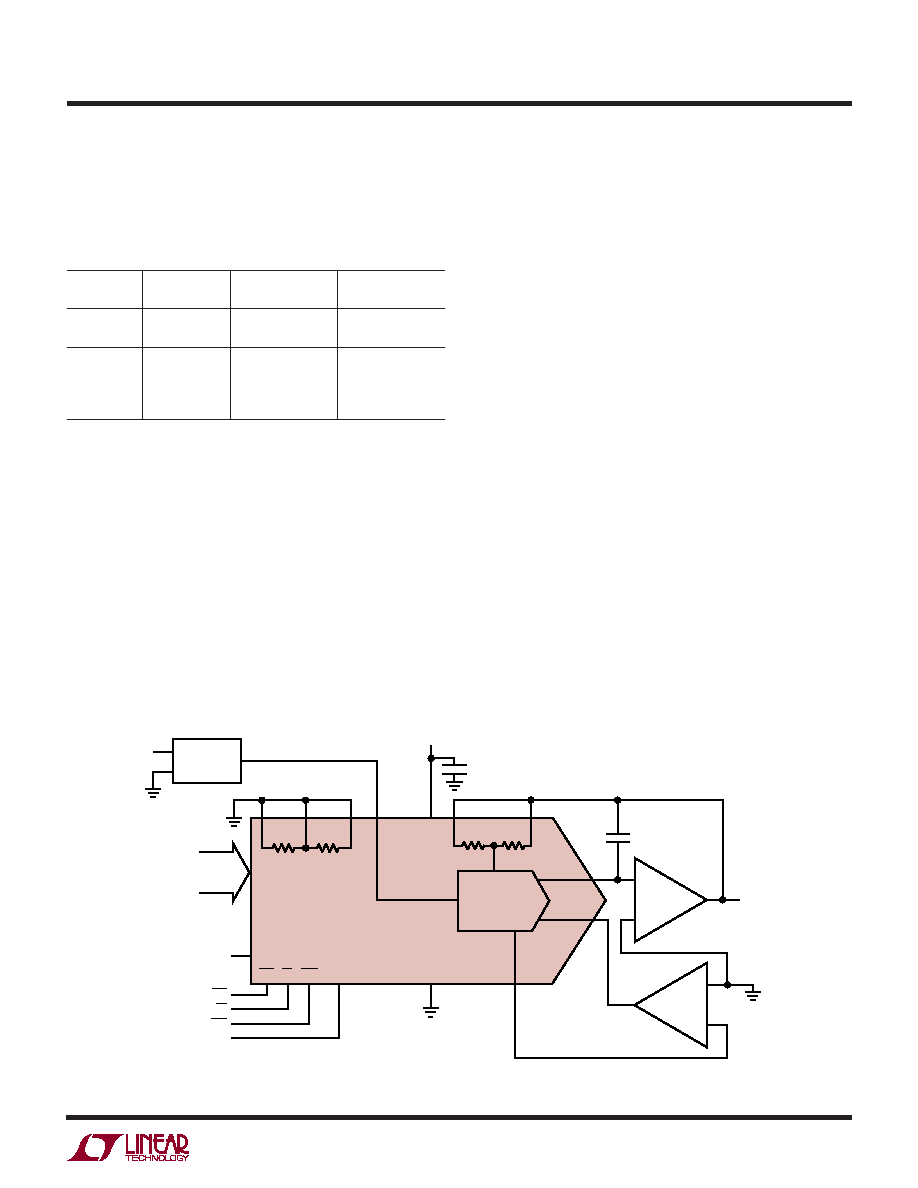
Grounding
As with any high resolution converter, clean grounding is
important. A low impedance analog ground plane and star
grounding should be used. IOUT2F and IOUT2S must be tied
to the star ground with as low a resistance as possible.
When it is not possible to locate star ground close to
IOUT2F and IOUT2S, separate traces should be used to route
these pins to star ground. This minimizes the voltage drop
from these pins to ground caused by the code dependent
current flowing to ground. When the resistance of these
circuit board traces becomes greater than 1, the circuit
in Figure 4 eliminates voltage drop errors caused by high
resistance traces. This preserves the excellent accuracy
(1LSB INL and DNL) of the LTC1599.
A 16-Bit, 4mA to 20mA Current Loop Controller
for Industrial Applications
Modern process control systems must often deal with
legacy 4mA to 20mA analog current loops as a means of
interfacing with actuators and valves located at a distance.
The circuit in Figure 5 provides an output to a current loop
controlled by an LTC1599, a 16-bit current output DAC. A
dual rail-to-rail op amp (U1, LT1366) controls a P-channel
power FET (Q2) to produce a current mirror with a precise
8:1 ratio as defined by a resistor array. The input current
to this mirror circuit is produced by a grounded base
cascode stage using a high gain transistor (Q1). The use
of a bipolar transistor in this location results in an error
term associated with U1B and Q1’s base current (– 0.2%
for the device shown). For control applications however,
absolute accuracy of the output to an actuator is usually
not required. If a higher degree of absolute accuracy is
required, Q1 can be replaced with an N-channel JFET;
however, this requires a single amplifier at U1B with the
ability to drive the gate below ground. An enhancement
mode N-channel FET can be used in place of Q1 but
MOSFET leakage current must be considered and gate
overdrive must be avoided.
Figure 4. Driving IOUT2F and IOUT2S with a Force/Sense Amplifier
VCC
LTC1599
RFB
ROFS
5V
4
3
20
8
R1
RCOM
2
R2
1
REF
5
6
0.1F
7
IOUT1
33pF
VOUT
0V TO –10V
1599 F04
–
+
LT1001
–
+
LT1001
16-BIT DAC
R1
R2
IOUT2F
IOUT2S
13
MLBYTE
14 TO 18,
21 TO 23
8
DATA
INPUTS
LD
12
11
24
10
WR
CLR
CLVL
CLR
19
9
DGND
CLVL
3
6
2
6
3
LT1236A-10
2
6 10V
15V
4
相关PDF资料 |
PDF描述 |
|---|---|
| VI-B3H-MU-S | CONVERTER MOD DC/DC 52V 200W |
| VI-240-IV | CONVERTER MOD DC/DC 5V 150W |
| VI-B1B-MX-S | CONVERTER MOD DC/DC 95V 75W |
| VI-B3F-MU-S | CONVERTER MOD DC/DC 72V 200W |
| LTC1599AIG | IC DAC 16BIT PARALLEL IN 24SSOP |
相关代理商/技术参数 |
参数描述 |
|---|---|
| LTC1599AIN | 功能描述:IC DAC 16BIT PARALLEL IN 24DIP RoHS:否 类别:集成电路 (IC) >> 数据采集 - 数模转换器 系列:- 产品培训模块:Lead (SnPb) Finish for COTS Obsolescence Mitigation Program 标准包装:1,000 系列:- 设置时间:1µs 位数:8 数据接口:串行 转换器数目:8 电压电源:双 ± 功率耗散(最大):941mW 工作温度:0°C ~ 70°C 安装类型:表面贴装 封装/外壳:24-SOIC(0.295",7.50mm 宽) 供应商设备封装:24-SOIC W 包装:带卷 (TR) 输出数目和类型:8 电压,单极 采样率(每秒):* |
| LTC1599AIN#PBF | 功能描述:IC D/A CONV 16BIT MLTPLYNG 24DIP RoHS:是 类别:集成电路 (IC) >> 数据采集 - 数模转换器 系列:- 标准包装:2,400 系列:- 设置时间:- 位数:18 数据接口:串行 转换器数目:3 电压电源:模拟和数字 功率耗散(最大):- 工作温度:-40°C ~ 85°C 安装类型:表面贴装 封装/外壳:36-TFBGA 供应商设备封装:36-TFBGA 包装:带卷 (TR) 输出数目和类型:* 采样率(每秒):* |
| LTC1599BCG | 功能描述:IC DAC 16BIT PARALLEL IN 24SSOP RoHS:否 类别:集成电路 (IC) >> 数据采集 - 数模转换器 系列:- 产品培训模块:Data Converter Fundamentals DAC Architectures 标准包装:750 系列:- 设置时间:7µs 位数:16 数据接口:并联 转换器数目:1 电压电源:双 ± 功率耗散(最大):100mW 工作温度:0°C ~ 70°C 安装类型:表面贴装 封装/外壳:28-LCC(J 形引线) 供应商设备封装:28-PLCC(11.51x11.51) 包装:带卷 (TR) 输出数目和类型:1 电压,单极;1 电压,双极 采样率(每秒):143k |
| LTC1599BCG#PBF | 功能描述:IC DAC 16BIT W/RES 24-SSOP RoHS:是 类别:集成电路 (IC) >> 数据采集 - 数模转换器 系列:- 产品培训模块:Data Converter Fundamentals DAC Architectures 标准包装:750 系列:- 设置时间:7µs 位数:16 数据接口:并联 转换器数目:1 电压电源:双 ± 功率耗散(最大):100mW 工作温度:0°C ~ 70°C 安装类型:表面贴装 封装/外壳:28-LCC(J 形引线) 供应商设备封装:28-PLCC(11.51x11.51) 包装:带卷 (TR) 输出数目和类型:1 电压,单极;1 电压,双极 采样率(每秒):143k |
| LTC1599BCG#TR | 功能描述:IC DAC 16BIT PARALLEL IN 24SSOP RoHS:否 类别:集成电路 (IC) >> 数据采集 - 数模转换器 系列:- 产品培训模块:Data Converter Fundamentals DAC Architectures 标准包装:750 系列:- 设置时间:7µs 位数:16 数据接口:并联 转换器数目:1 电压电源:双 ± 功率耗散(最大):100mW 工作温度:0°C ~ 70°C 安装类型:表面贴装 封装/外壳:28-LCC(J 形引线) 供应商设备封装:28-PLCC(11.51x11.51) 包装:带卷 (TR) 输出数目和类型:1 电压,单极;1 电压,双极 采样率(每秒):143k |
发布紧急采购,3分钟左右您将得到回复。