- 您现在的位置:买卖IC网 > PDF目录2004 > LTC1599AIG#TRPBF (Linear Technology)IC D/A CONV 16BIT MLTPLYNG24SSOP PDF资料下载
参数资料
| 型号: | LTC1599AIG#TRPBF |
| 厂商: | Linear Technology |
| 文件页数: | 6/20页 |
| 文件大小: | 0K |
| 描述: | IC D/A CONV 16BIT MLTPLYNG24SSOP |
| 标准包装: | 1,800 |
| 设置时间: | 1µs |
| 位数: | 16 |
| 数据接口: | 并联 |
| 转换器数目: | 1 |
| 电压电源: | 单电源 |
| 功率耗散(最大): | 55µW |
| 工作温度: | -40°C ~ 85°C |
| 安装类型: | 表面贴装 |
| 封装/外壳: | 24-SSOP(0.209",5.30mm 宽) |
| 供应商设备封装: | 24-SSOP |
| 包装: | 带卷 (TR) |
| 输出数目和类型: | 3 电流,单极;3 电流,双极 |
| 采样率(每秒): | * |
14
LTC1599
sn1599 1599fs
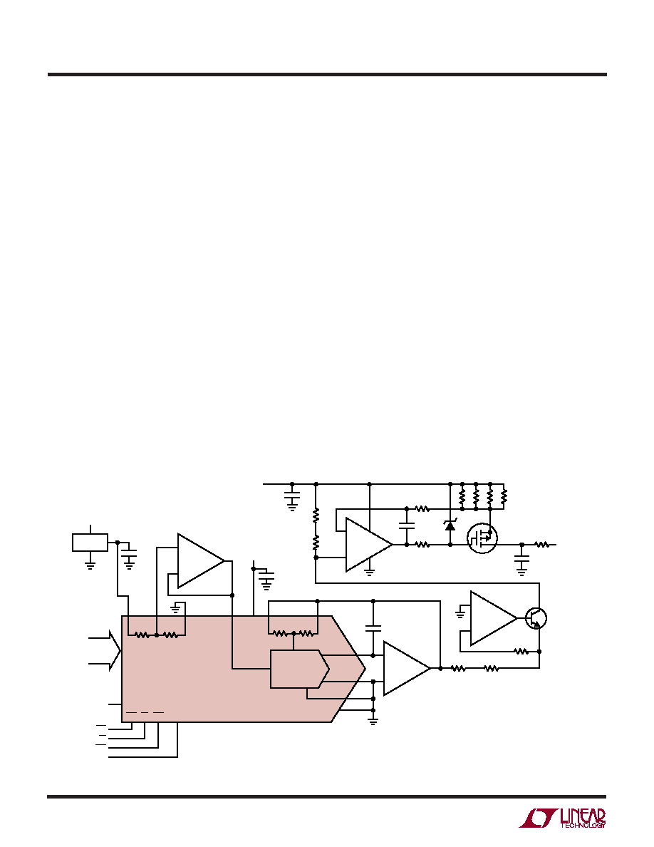
The output current of the DAC is converted to a voltage via
U3 (LT1112), producing 0V to – 2.5V at Pin 1 of U3. The
resulting current in Q1 is determined by two elements of
resistor array, RN1 (3mA max). The emitter of Q1 is
maintained at 0V by the action of U1B.
In applications that do not require 16-bit resolution and
accuracy, the LTC1599 can be replaced by the 14-bit
parallel LTC1591. Furthermore, the resistor array can be
substituted with discrete resistors, and Q2 could be re-
placed by a high gain bipolar PNP; for example, an FZT600
from Zetex.
No trim is provided a shown, as it is expected that software
control is preferable. The output range of 4mA to 20mA is
defined by software, as the full output range is nominally
0mA to 24mA.
U1 is a rail-to-rail amplifier that can operate on suppy
voltages up to 36V. This defines the maximum voltage on
the loop power. If higher loop voltages are required, a
separate low power amplifier at U1A, powered by a zener
regulated supply and referenced to loop power, would
allow voltages up to the breakdown voltages of Q1 and Q2.
APPLICATIONS INFORMATION
WU
U
In the example shown, the use of a dual op amp requires
a zener clamp to protect the gate of the MOS power
transistor. If a separate shunt-regulated supply is pro-
vided for the amplifier replacing U1A, the gate clamp (Z1)
is not required.
As shown, this topology uses the LTC1599’s internal
divider (R1 and R2) to reduce the reference from 5V to
2.5V. If a 2.5V reference is used, it can be connected
directly to REF (Pin 1). Alternatively, if the op amp is
powered such that it has –10V output capability, the
divider and amplifier prior to the REF input are not required
and ROFS can be used for other purposes such as offset
trim. The two RN1 resistors at the emitter of Q1 must be
changed in this case.
Note that the output of the current transmitter shows a
network that is intended to provide a first line of defense
against ESD and prevent oscillation (1000pF and 10)
that could otherwise occur in the power MOSFET if lead
inductance were more than a few inches. C1 should be as
close as possible to Q2. Using MOSFETs that have higher
threshold voltages may require changing Z1 in order to
allow full current output.
VCC
U2
LTC1599
RFB
ROFS
5V
7
5
6
0.1F
12
IF 2.5V REF USED CONNECT
DIRECTLY TO REF
4
3
20
8
R1
RCOM
2
R2
1
REF
5
6
0.1F
RN1
7
10
7
IOUT1
C3
33pF
–
+
U3
1/2 LT1112
–
+
U1B
1/2 LT1366
–
+
U1A
1/2 LT1366
16-BIT DAC
R1
R2
RN1
15
2
24V
2
8
1
4
3
C2
100pF
Z1
6.2V
RN1
LOOP POWER
0.1F
C1
1000pF
IOUT
Q2
Si9407AEX
IOUT2F
IOUT2S
13
MLBYTE
14 TO 18,
21 TO 23
8
DATA
INPUTS
LD
12
11
24
10
WR
CLR
CLVL
CLR
19
9
DGND
CLVL
3
1
RN1 = 400 × 8 RESISTOR ARRAY
116
RN1
98
5
6
7
RN1
R4
1k
R5
10
R3
1k
3
14
4
13
5
12
6
11
R6
1k
Q1
MMBT6429
HFE = 500
2
–
+
1/2 LT1112
LT1460-5
Figure 5. 16-Bit Current Loop Controller for Industrial Applications
相关PDF资料 |
PDF描述 |
|---|---|
| LTC1603IG#TRPBF | IC ADC W/SHUTDOWN 16BIT 36-SSOP |
| LTC1604AIG#TR | IC ADC 16BIT SAMPL SHTDWN 36SSOP |
| LTC1605-1IN#PBF | IC A/D CONV 16BIT SAMPLNG 28-DIP |
| LTC1605AISW#TR | IC ADC 16BIT 5V SAMPLING 28SOIC |
| LTC1606AISW#TRPBF | IC A/D CONV 16BIT SAMPLNG 28SOIC |
相关代理商/技术参数 |
参数描述 |
|---|---|
| LTC1599AIN | 功能描述:IC DAC 16BIT PARALLEL IN 24DIP RoHS:否 类别:集成电路 (IC) >> 数据采集 - 数模转换器 系列:- 产品培训模块:Lead (SnPb) Finish for COTS Obsolescence Mitigation Program 标准包装:1,000 系列:- 设置时间:1µs 位数:8 数据接口:串行 转换器数目:8 电压电源:双 ± 功率耗散(最大):941mW 工作温度:0°C ~ 70°C 安装类型:表面贴装 封装/外壳:24-SOIC(0.295",7.50mm 宽) 供应商设备封装:24-SOIC W 包装:带卷 (TR) 输出数目和类型:8 电压,单极 采样率(每秒):* |
| LTC1599AIN#PBF | 功能描述:IC D/A CONV 16BIT MLTPLYNG 24DIP RoHS:是 类别:集成电路 (IC) >> 数据采集 - 数模转换器 系列:- 标准包装:2,400 系列:- 设置时间:- 位数:18 数据接口:串行 转换器数目:3 电压电源:模拟和数字 功率耗散(最大):- 工作温度:-40°C ~ 85°C 安装类型:表面贴装 封装/外壳:36-TFBGA 供应商设备封装:36-TFBGA 包装:带卷 (TR) 输出数目和类型:* 采样率(每秒):* |
| LTC1599BCG | 功能描述:IC DAC 16BIT PARALLEL IN 24SSOP RoHS:否 类别:集成电路 (IC) >> 数据采集 - 数模转换器 系列:- 产品培训模块:Data Converter Fundamentals DAC Architectures 标准包装:750 系列:- 设置时间:7µs 位数:16 数据接口:并联 转换器数目:1 电压电源:双 ± 功率耗散(最大):100mW 工作温度:0°C ~ 70°C 安装类型:表面贴装 封装/外壳:28-LCC(J 形引线) 供应商设备封装:28-PLCC(11.51x11.51) 包装:带卷 (TR) 输出数目和类型:1 电压,单极;1 电压,双极 采样率(每秒):143k |
| LTC1599BCG#PBF | 功能描述:IC DAC 16BIT W/RES 24-SSOP RoHS:是 类别:集成电路 (IC) >> 数据采集 - 数模转换器 系列:- 产品培训模块:Data Converter Fundamentals DAC Architectures 标准包装:750 系列:- 设置时间:7µs 位数:16 数据接口:并联 转换器数目:1 电压电源:双 ± 功率耗散(最大):100mW 工作温度:0°C ~ 70°C 安装类型:表面贴装 封装/外壳:28-LCC(J 形引线) 供应商设备封装:28-PLCC(11.51x11.51) 包装:带卷 (TR) 输出数目和类型:1 电压,单极;1 电压,双极 采样率(每秒):143k |
| LTC1599BCG#TR | 功能描述:IC DAC 16BIT PARALLEL IN 24SSOP RoHS:否 类别:集成电路 (IC) >> 数据采集 - 数模转换器 系列:- 产品培训模块:Data Converter Fundamentals DAC Architectures 标准包装:750 系列:- 设置时间:7µs 位数:16 数据接口:并联 转换器数目:1 电压电源:双 ± 功率耗散(最大):100mW 工作温度:0°C ~ 70°C 安装类型:表面贴装 封装/外壳:28-LCC(J 形引线) 供应商设备封装:28-PLCC(11.51x11.51) 包装:带卷 (TR) 输出数目和类型:1 电压,单极;1 电压,双极 采样率(每秒):143k |
发布紧急采购,3分钟左右您将得到回复。