参数资料
| 型号: | LTC1599BCG#TR |
| 厂商: | Linear Technology |
| 文件页数: | 2/20页 |
| 文件大小: | 0K |
| 描述: | IC DAC 16BIT PARALLEL IN 24SSOP |
| 标准包装: | 1,800 |
| 设置时间: | 1µs |
| 位数: | 16 |
| 数据接口: | 并联 |
| 转换器数目: | 1 |
| 电压电源: | 单电源 |
| 功率耗散(最大): | 55µW |
| 工作温度: | 0°C ~ 70°C |
| 安装类型: | 表面贴装 |
| 封装/外壳: | 24-SSOP(0.209",5.30mm 宽) |
| 供应商设备封装: | 24-SSOP |
| 包装: | 带卷 (TR) |
| 输出数目和类型: | 3 电流,单极;3 电流,双极 |
| 采样率(每秒): | * |
10
LTC1599
sn1599 1599fs
APPLICATIONS INFORMATION
WU
U
configured in unipolar or bipolar modes of operation
(Figures 1 and 3). These are the changes the op amp can
cause to the INL, DNL, unipolar offset, unipolar gain error,
bipolar zero and bipolar gain error. Table 4 contains a
partial list of LTC precision op amps recommended for use
with the LTC1599. The two sets of easy-to-use design
equations simplify the selection of op amps to meet the
system’s specified error budget. Select the amplifier from
Table 4 and insert the specified op amp parameters in
either Table 2 or Table 3. Add up all the errors for each
category to determine the effect the op amp has on the
accuracy of the LTC1599. Arithmetic summation gives an
(unlikely) worst-case effect. RMS summation produces a
more realistic effect.
Op amp offset will contribute mostly to output offset and
gain error and has minimal effect on INL and DNL. For the
LTC1599, a 500V op amp offset will cause about 0.55LSB
INL degradation and 0.15LSB DNL degradation with a 10V
full-scale range (20V range in bipolar). For the LTC1599
configured in the unipolar mode, the same 500V op amp
offset will cause a 3.3LSB zero-scale error and a 3.45LSB
gain error with a 10V full-scale range.
While not directly addressed by the simple equations in
Tables 2 and 3, temperature effects can be handled just as
easily for unipolar and bipolar applications. First, consult
an op amp’s data sheet to find the worst-case VOS and IB
over temperature. Then, plug these numbers in the VOS
and IB equations from Table 2 or Table 3 and calculate the
temperature induced effects.
For applications where fast settling time is important,
Application Note 74, entitled “
Component and Measure-
ment Advances Ensure 16-Bit DAC Settling Time,” offers
a thorough discussion of 16-bit DAC settling time and op
amp selection.
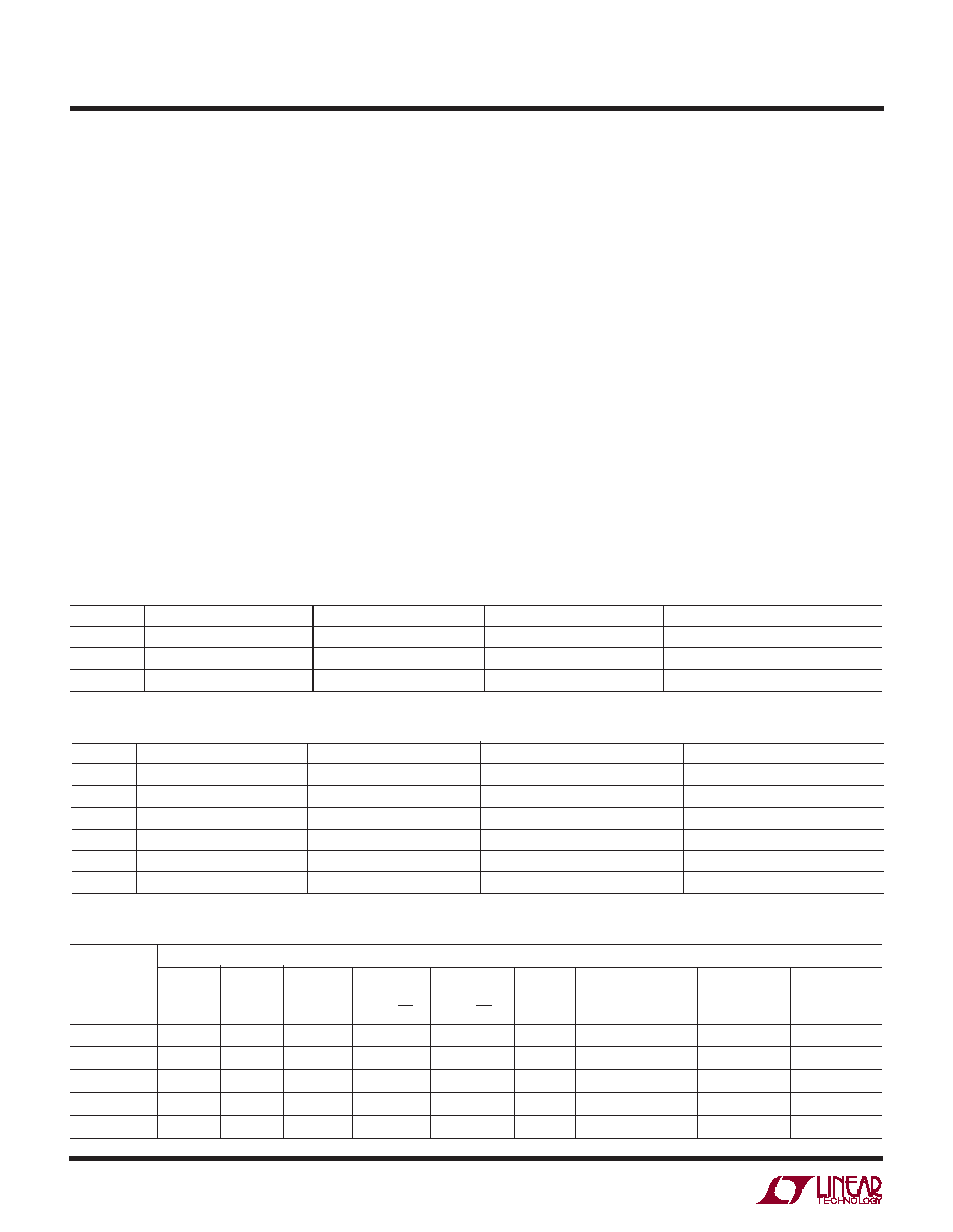
Table 4. Partial List of LTC Precision Amplifiers Recommended for Use with the LTC1599, with Relevant Specifications
Amplifier Specifications
VOLTAGE
CURRENT
SLEW
GAIN BANDWIDTH
tSETTLING
POWER
VOS
IB
AOL
NOISE
RATE
PRODUCT
with LTC1599
DISSIPATION
AMPLIFIER
V
nA
V/mV
nV/√Hz
pA/√Hz
V/s
MHz
smW
LT1001
25
2
800
10
0.12
0.25
0.8
120
46
LT1097
50
0.35
1000
14
0.008
0.2
0.7
120
11
LT1112 (Dual)
60
0.25
1500
14
0.008
0.16
0.75
115
10.5/Op Amp
LT1124 (Dual)
70
20
4000
2.7
0.3
4.5
12.5
19
69/Op Amp
LT1468
75
10
5000
5
0.6
22
90
2.5
117
Table 2. Easy-to-Use Equations Determine Op Amp Effects on DAC Accuracy in Unipolar Applications
OP AMP
INL (LSB)
DNL (LSB)
UNIPOLAR OFFSET (LSB)
UNIPOLAR GAIN ERROR (LSB)
VOS (mV)
VOS 1.2 (10V/VREF)VOS 0.3 (10V/VREF)VOS 6.6 (10V/VREF)VOS 6.9 (10V/VREF)
IB (nA)
IB 0.00055 (10V/VREF)IB 0.00015 (10V/VREF)IB 0.065 (10V/VREF)0
AVOL (V/V)
10k/AVOL
3k/AVOL
0
131k/AVOL
Table 3. Easy-to-Use Equations Determine Op Amp Effects on DAC Accuracy in Bipolar Applications
OP AMP
INL (LSB)
DNL (LSB)
BIPOLAR ZERO ERROR (LSB)
BIPOLAR GAIN ERROR (LSB)
VOS1 (mV)
VOS1 1.2 (10V/VREF)VOS1 0.3 (10V/VREF)VOS1 9.9 (10V/VREF)VOS1 6.9 (10V/VREF)
IB1 (nA)
IB1 0.00055 (10V/VREF)IB1 0.00015 (10V/VREF)IB1 0.065 (10V/VREF)0
AVOL1
10k/AVOL
3k/AVOL1
0
196k/AVOL1
VOS2 (mV)
0
VOS2 6.7 (10V/VREF)VOS2 13.2 (10V/VREF)
IB2 (nA)
0
IB2 0.065 (10V/VREF)IB2 0.13 (10V/VREF)
AVOL2
0
65k/AVOL2
131k/AVOL2
相关PDF资料 |
PDF描述 |
|---|---|
| VI-B3H-MY-B1 | CONVERTER MOD DC/DC 52V 50W |
| VI-B3D-MY-B1 | CONVERTER MOD DC/DC 85V 50W |
| VI-B3B-MW-B1 | CONVERTER MOD DC/DC 95V 100W |
| VI-253-IV-F2 | CONVERTER MOD DC/DC 24V 150W |
| VI-B34-MY-B1 | CONVERTER MOD DC/DC 48V 50W |
相关代理商/技术参数 |
参数描述 |
|---|---|
| LTC1599BCN | 功能描述:IC DAC 16BIT PARALLEL IN 24DIP RoHS:否 类别:集成电路 (IC) >> 数据采集 - 数模转换器 系列:- 产品培训模块:Data Converter Fundamentals DAC Architectures 标准包装:750 系列:- 设置时间:7µs 位数:16 数据接口:并联 转换器数目:1 电压电源:双 ± 功率耗散(最大):100mW 工作温度:0°C ~ 70°C 安装类型:表面贴装 封装/外壳:28-LCC(J 形引线) 供应商设备封装:28-PLCC(11.51x11.51) 包装:带卷 (TR) 输出数目和类型:1 电压,单极;1 电压,双极 采样率(每秒):143k |
| LTC1599BCN#PBF | 功能描述:IC D/A CONV 16BIT MLTPLYNG 24DIP RoHS:是 类别:集成电路 (IC) >> 数据采集 - 数模转换器 系列:- 标准包装:2,400 系列:- 设置时间:- 位数:18 数据接口:串行 转换器数目:3 电压电源:模拟和数字 功率耗散(最大):- 工作温度:-40°C ~ 85°C 安装类型:表面贴装 封装/外壳:36-TFBGA 供应商设备封装:36-TFBGA 包装:带卷 (TR) 输出数目和类型:* 采样率(每秒):* |
| LTC1599BIG | 功能描述:IC DAC 16BIT PARALLEL IN 24SSOP RoHS:否 类别:集成电路 (IC) >> 数据采集 - 数模转换器 系列:- 产品培训模块:Data Converter Fundamentals DAC Architectures 标准包装:750 系列:- 设置时间:7µs 位数:16 数据接口:并联 转换器数目:1 电压电源:双 ± 功率耗散(最大):100mW 工作温度:0°C ~ 70°C 安装类型:表面贴装 封装/外壳:28-LCC(J 形引线) 供应商设备封装:28-PLCC(11.51x11.51) 包装:带卷 (TR) 输出数目和类型:1 电压,单极;1 电压,双极 采样率(每秒):143k |
| LTC1599BIG#PBF | 功能描述:IC D/A CONV 16BIT MLTPLYNG24SSOP RoHS:是 类别:集成电路 (IC) >> 数据采集 - 数模转换器 系列:- 产品培训模块:Data Converter Fundamentals DAC Architectures 标准包装:750 系列:- 设置时间:7µs 位数:16 数据接口:并联 转换器数目:1 电压电源:双 ± 功率耗散(最大):100mW 工作温度:0°C ~ 70°C 安装类型:表面贴装 封装/外壳:28-LCC(J 形引线) 供应商设备封装:28-PLCC(11.51x11.51) 包装:带卷 (TR) 输出数目和类型:1 电压,单极;1 电压,双极 采样率(每秒):143k |
| LTC1599BIG#TR | 功能描述:IC DAC 16BIT PARALLEL IN 24SSOP RoHS:否 类别:集成电路 (IC) >> 数据采集 - 数模转换器 系列:- 产品培训模块:Data Converter Fundamentals DAC Architectures 标准包装:750 系列:- 设置时间:7µs 位数:16 数据接口:并联 转换器数目:1 电压电源:双 ± 功率耗散(最大):100mW 工作温度:0°C ~ 70°C 安装类型:表面贴装 封装/外壳:28-LCC(J 形引线) 供应商设备封装:28-PLCC(11.51x11.51) 包装:带卷 (TR) 输出数目和类型:1 电压,单极;1 电压,双极 采样率(每秒):143k |
发布紧急采购,3分钟左右您将得到回复。