- 您现在的位置:买卖IC网 > PDF目录10168 > LTC1605-2CG#TR (Linear Technology)IC ADC 16BIT 5V SAMPLING 28SSOP PDF资料下载
参数资料
| 型号: | LTC1605-2CG#TR |
| 厂商: | Linear Technology |
| 文件页数: | 19/20页 |
| 文件大小: | 0K |
| 描述: | IC ADC 16BIT 5V SAMPLING 28SSOP |
| 标准包装: | 2,000 |
| 位数: | 16 |
| 采样率(每秒): | 100k |
| 数据接口: | 并联 |
| 转换器数目: | 1 |
| 功率耗散(最大): | 80mW |
| 电压电源: | 模拟和数字 |
| 工作温度: | 0°C ~ 70°C |
| 安装类型: | 表面贴装 |
| 封装/外壳: | 28-SSOP(0.209",5.30mm 宽) |
| 供应商设备封装: | 28-SSOP |
| 包装: | 带卷 (TR) |
| 输入数目和类型: | 1 个单端,双极 |
| 配用: | DC1255A-A-ND - BOARD SAR ADC LTC1605 |
8
LTC1605-1/LTC1605-2
APPLICATIONS INFORMATION
WU
U
LT
1007 - Low noise precision amplifier. 2.7mA supply
current
±5V to ±15V supplies. Gain bandwidth product
8MHz. DC applications.
LT1097 - Low cost, low power precision amplifier. 300
A
supply current.
±5V to ±15V supplies. Gain bandwidth
product 0.7MHz. DC applications.
LT1227 - 140MHz video current feedback amplifier.
10mA supply current.
±5V to ±15V supplies. Low noise
and low distortion.
LT1360 - 37MHz voltage feedback amplifier. 3.8mA
supply current.
±5V to ±15V supplies. Good AC/DC
specs.
LT1363 - 50MHz voltage feedback amplifier. 6.3mA
supply current. Good AC/DC specs.
LT1364/LT1365 - Dual and quad 50MHz voltage feed-
back amplifiers. 6.3mA supply current per amplifier.
Good AC/DC specs.
LT1468 - 90MHz, 22V/
s 16-Bit Accurate Amplifier
For minimum code transition noise the REF pin and the
CAP pin should each be decoupled with a capacitor to
filter wideband noise from the reference and the buffer
(2.2
F tantalum).
Offset and Gain Adjustments
The LTC1605-1/LTC1605-2 offset and full-scale errors
have been trimmed at the factory with the external
resistors shown in Figure 4. This allows for external
adjustment of offset and full scale in applications where
absolute accuracy is important. See Figure 5 for the offset
and gain trim circuit for the LTC1605-1/LTC1605-2.
First adjust the offset to zero by adjusting resistor R3.
Apply an input voltage of 30.5
V (0.5LSB) and adjust R3
so the code is changing between 0000 0000 0000 0001
and 0000 0000 0000 0000. The gain error is trimmed by
adjusting resistor R4. An input voltage of 3.999908V (FS
– 1.5LSB) is applied to VIN and R4 is adjusted until the
output code is changing between 1111 1111 1111 1110
and 1111 1111 1111 1111. Figure 6a shows the unipolar
transfer characteristic of the LTC1605-1.
For the LTC1605-2, first adjust the offset to zero by
adjusting resistor R3. Apply an input voltage of – 61
V
(– 0.5LSB) and adjust R3 so the code is changing be-
tween 1111 1111 1111 1111 and 0000 0000 0000 0000.
The gain error is trimmed by adjusting resistor R4. An
input voltage of 3.999817V (+ FS – 1.5LSB) is applied to
VIN and R4 is adjusted until the outut code is changing
between 0111 1111 1111 1110 and 0111 1111 1111
1111. Figure 6b shows the bipolar transfer characteris-
tics of the LTC1605-2.
DC Performance
One way of measuring the transition noise associated
with a high resolution ADC is to use a technique where a
DC signal is applied to the input of the ADC and the
resulting output codes are collected over a large number
of conversions. For example, in Figure 7 the distribution
of output code is shown for a DC input that has been
digitized 10000 times. The distribution is Gaussian and
the RMS code transition is about 1LSB.
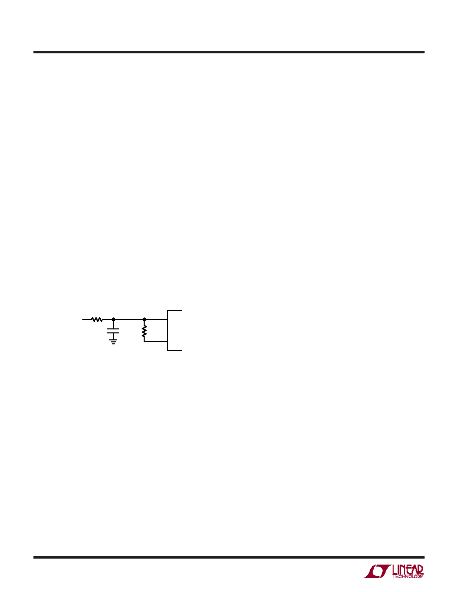
Figure 2. Analog Input Filtering
1605-1/2 F02
1000pF
33.2k
VIN
CAP
AIN
200
Internal Voltage Reference
The LTC1605-1/LTC1605-2 has an on-chip, temperature
compensated, curvature corrected, bandgap reference,
which is factory trimmed to 2.50V. The full-scale range of
the ADC is equal to (1.6VREF) or nominally 0V to 4V for the
LTC1605-1 and (
±1.6VREF) or nominally ±4V for the
LTC1605-2. The output of the reference is connected to
the input of a unity-gain buffer through a 4k resistor (see
Figure 3). The input to the buffer or the output of the
reference is available at REF (Pin 3). The internal refer-
ence can be overdriven with an external reference if more
accuracy is needed. The buffer output drives the internal
DAC and is available at CAP (Pin 4). The CAP pin can be
used to drive a steady DC load of less than 2mA. Driving
an AC load is not recommended because it can cause the
performance of the converter to degrade.
相关PDF资料 |
PDF描述 |
|---|---|
| IDT72V265LA10PFG | IC FIFO SS 16384X18 10NS 64-TQFP |
| VI-26H-IW-S | CONVERTER MOD DC/DC 52V 100W |
| VI-B73-MY | CONVERTER MOD DC/DC 24V 50W |
| IDT7208L20J | IC FIFO 64KX9 20NS 32PLCC |
| VI-B72-MY | CONVERTER MOD DC/DC 15V 50W |
相关代理商/技术参数 |
参数描述 |
|---|---|
| LTC1605-2CN | 功能描述:IC ADC 16BIT 5V SAMPLING 28DIP RoHS:否 类别:集成电路 (IC) >> 数据采集 - 模数转换器 系列:- 标准包装:1,000 系列:- 位数:12 采样率(每秒):300k 数据接口:并联 转换器数目:1 功率耗散(最大):75mW 电压电源:单电源 工作温度:0°C ~ 70°C 安装类型:表面贴装 封装/外壳:24-SOIC(0.295",7.50mm 宽) 供应商设备封装:24-SOIC 包装:带卷 (TR) 输入数目和类型:1 个单端,单极;1 个单端,双极 |
| LTC1605-2CN#PBF | 功能描述:IC A/D CONV 16BIT SAMPLNG 28-DIP RoHS:是 类别:集成电路 (IC) >> 数据采集 - 模数转换器 系列:- 标准包装:1,000 系列:- 位数:12 采样率(每秒):300k 数据接口:并联 转换器数目:1 功率耗散(最大):75mW 电压电源:单电源 工作温度:0°C ~ 70°C 安装类型:表面贴装 封装/外壳:24-SOIC(0.295",7.50mm 宽) 供应商设备封装:24-SOIC 包装:带卷 (TR) 输入数目和类型:1 个单端,单极;1 个单端,双极 |
| LTC1605-2IG | 功能描述:IC A/D CONV 16BIT SAMPLNG 28SSOP RoHS:否 类别:集成电路 (IC) >> 数据采集 - 模数转换器 系列:- 标准包装:1,000 系列:- 位数:12 采样率(每秒):300k 数据接口:并联 转换器数目:1 功率耗散(最大):75mW 电压电源:单电源 工作温度:0°C ~ 70°C 安装类型:表面贴装 封装/外壳:24-SOIC(0.295",7.50mm 宽) 供应商设备封装:24-SOIC 包装:带卷 (TR) 输入数目和类型:1 个单端,单极;1 个单端,双极 |
| LTC1605-2IG#PBF | 功能描述:IC A/D CONV 16BIT SAMPLNG 28SSOP RoHS:是 类别:集成电路 (IC) >> 数据采集 - 模数转换器 系列:- 标准包装:1,000 系列:- 位数:12 采样率(每秒):300k 数据接口:并联 转换器数目:1 功率耗散(最大):75mW 电压电源:单电源 工作温度:0°C ~ 70°C 安装类型:表面贴装 封装/外壳:24-SOIC(0.295",7.50mm 宽) 供应商设备封装:24-SOIC 包装:带卷 (TR) 输入数目和类型:1 个单端,单极;1 个单端,双极 |
| LTC1605-2IG#TR | 功能描述:IC ADC 16BIT 5V SAMPLING 28SSOP RoHS:否 类别:集成电路 (IC) >> 数据采集 - 模数转换器 系列:- 标准包装:1,000 系列:- 位数:12 采样率(每秒):300k 数据接口:并联 转换器数目:1 功率耗散(最大):75mW 电压电源:单电源 工作温度:0°C ~ 70°C 安装类型:表面贴装 封装/外壳:24-SOIC(0.295",7.50mm 宽) 供应商设备封装:24-SOIC 包装:带卷 (TR) 输入数目和类型:1 个单端,单极;1 个单端,双极 |
发布紧急采购,3分钟左右您将得到回复。