- 您现在的位置:买卖IC网 > PDF目录2004 > LTC1606AISW#TRPBF (Linear Technology)IC A/D CONV 16BIT SAMPLNG 28SOIC PDF资料下载
参数资料
| 型号: | LTC1606AISW#TRPBF |
| 厂商: | Linear Technology |
| 文件页数: | 2/16页 |
| 文件大小: | 0K |
| 描述: | IC A/D CONV 16BIT SAMPLNG 28SOIC |
| 标准包装: | 1,000 |
| 位数: | 16 |
| 采样率(每秒): | 250k |
| 数据接口: | 并联 |
| 转换器数目: | 1 |
| 功率耗散(最大): | 100mW |
| 电压电源: | 模拟和数字 |
| 工作温度: | -40°C ~ 85°C |
| 安装类型: | 表面贴装 |
| 封装/外壳: | 28-SOIC(0.295",7.50mm 宽) |
| 供应商设备封装: | 28-SOIC |
| 包装: | 带卷 (TR) |
| 输入数目和类型: | 1 个单端,双极 |
10
LTC1606
1606fa
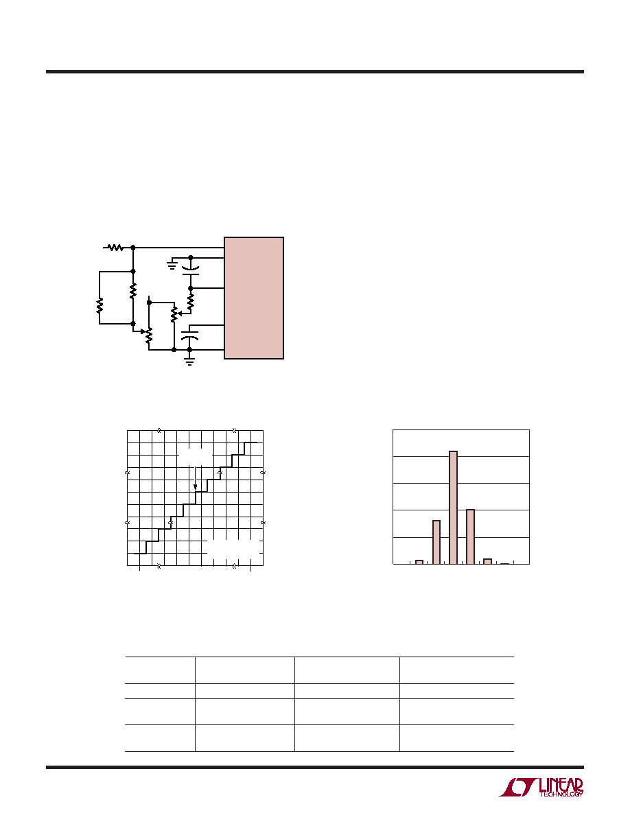
changing between 1111 1111 1111 1111 and 0000 0000
0000 0000. The gain error is trimmed by adjusting resistor
R4. An input voltage of 9.999542V (+FS – 1.5LSB) is
applied to VIN and R4 is adjusted until the output code is
changing between 0111 1111 1111 1110 and 0111 1111
1111 1111. Figure 6 shows the bipolar transfer character-
istic of the LTC1606.
If the external resistors are not used, the resulting offset
and gain error ranges are shown in Table 1.
DC Performance
One way of measuring the transition noise associated with
a high resolution ADC is to use a technique where a DC
signal is applied to the input of the ADC and the resulting
output codes are collected over a large number of conver-
sions. For example in Figure 7, the distribution of output
code is shown for a DC input that has been digitized 4096
times. The distribution is Gaussian and the RMS code
transition is about 0.65LSB.
DIGITAL INTERFACE
Internal Clock
The ADC has an internal clock that is trimmed to achieve
a typical conversion time of 2.3
s. No external adjust-
ments are required and, with the typical acquisition time of
1
s, throughput performance of 250ksps is assured.
+
5
4
3
2
1
10
F
+
2.2
F
33.2k
1%
100k
±10V INPUT
200
1%
VIN
AGND1
REF
CAP
AGND2
LTC1606
1606 F05
392k
R4
50k
R3
50k
5V
Figure 5.
±10V Input with Offset and Gain Trim
INPUT VOLTAGE (V)
0V
OUTPUT
CODE
–1
LSB
1606 F06
011...111
011...110
000...001
000...000
100...000
100...001
111...110
1
LSB
BIPOLAR
ZERO
111...111
FS/2 – 1LSB
–FS/2
FS = 20V
1LSB = FS/65536
Figure 6. LTC1606 Bipolar Transfer Characteristics
Table 1
WITH BOTH EXTERNAL
WITHOUT THE EXTERNAL
WITHOUT EITHER EXTERNAL
ERROR TERM
RESISTORS INCLUDED
33.2k RESISTOR
RESISTOR INCLUDED
Offset Error
– 10mV < Error < 10mV
10mV < Error< 55mV
54mV < Error < 155mV
+ Full-Scale Error
– 0.25% < Error < 0.25%
– 0.50% < Error < 0.50%
– 1.3% < Error < –0.10%
– 3.40% < Error < –0.85%
– Full-Scale Error
– 0.25% < Error < 0.25%
– 0.50% < Error < 0.50%
0.25% < Error < 1.40%
2.10% < Error < 6.15%
APPLICATIO S I FOR ATIO
WU
UU
Figure 7. Histogram for 4096 Conversions
2500
2000
1500
1000
500
0
–3
–2
–1
0
1
2
3
4
COUNTS
CODE
1606 F07
相关PDF资料 |
PDF描述 |
|---|---|
| LTC1608AIG#TRPBF | IC A/D CONV 16BIT SAMPLNG 36SSOP |
| LTC1609IG | IC A/D CONV 16BIT SAMPLNG 28SSOP |
| LTC1650AIS#TRPBF | IC D/A CONV 16BIT R-R 16-SOIC |
| LTC1654IGN#TR | IC DAC 14BIT DUAL R-R 16SSOP |
| LTC1655LIS8#TRPBF | IC DAC 16BIT R-R MICROPWR 8SOIC |
相关代理商/技术参数 |
参数描述 |
|---|---|
| LTC1606CG | 功能描述:IC ADC 16BIT 5V SAMPLING 28SSOP RoHS:否 类别:集成电路 (IC) >> 数据采集 - 模数转换器 系列:- 标准包装:1 系列:- 位数:14 采样率(每秒):83k 数据接口:串行,并联 转换器数目:1 功率耗散(最大):95mW 电压电源:双 ± 工作温度:0°C ~ 70°C 安装类型:通孔 封装/外壳:28-DIP(0.600",15.24mm) 供应商设备封装:28-PDIP 包装:管件 输入数目和类型:1 个单端,双极 |
| LTC1606CG#PBF | 功能描述:IC ADC 16BIT SMPL 250KSPS 28SSOP RoHS:是 类别:集成电路 (IC) >> 数据采集 - 模数转换器 系列:- 标准包装:1 系列:- 位数:14 采样率(每秒):83k 数据接口:串行,并联 转换器数目:1 功率耗散(最大):95mW 电压电源:双 ± 工作温度:0°C ~ 70°C 安装类型:通孔 封装/外壳:28-DIP(0.600",15.24mm) 供应商设备封装:28-PDIP 包装:管件 输入数目和类型:1 个单端,双极 |
| LTC1606CG#TR | 功能描述:IC ADC 16BIT 5V SAMPLING 28SSOP RoHS:否 类别:集成电路 (IC) >> 数据采集 - 模数转换器 系列:- 标准包装:1 系列:- 位数:14 采样率(每秒):83k 数据接口:串行,并联 转换器数目:1 功率耗散(最大):95mW 电压电源:双 ± 工作温度:0°C ~ 70°C 安装类型:通孔 封装/外壳:28-DIP(0.600",15.24mm) 供应商设备封装:28-PDIP 包装:管件 输入数目和类型:1 个单端,双极 |
| LTC1606CG#TRPBF | 功能描述:IC A/D CONV 16BIT SAMPLNG 28SSOP RoHS:是 类别:集成电路 (IC) >> 数据采集 - 模数转换器 系列:- 标准包装:1 系列:- 位数:14 采样率(每秒):83k 数据接口:串行,并联 转换器数目:1 功率耗散(最大):95mW 电压电源:双 ± 工作温度:0°C ~ 70°C 安装类型:通孔 封装/外壳:28-DIP(0.600",15.24mm) 供应商设备封装:28-PDIP 包装:管件 输入数目和类型:1 个单端,双极 |
| LTC1606CSW | 功能描述:IC ADC 16BIT 5V SAMPLING 28SOIC RoHS:否 类别:集成电路 (IC) >> 数据采集 - 模数转换器 系列:- 标准包装:1 系列:- 位数:14 采样率(每秒):83k 数据接口:串行,并联 转换器数目:1 功率耗散(最大):95mW 电压电源:双 ± 工作温度:0°C ~ 70°C 安装类型:通孔 封装/外壳:28-DIP(0.600",15.24mm) 供应商设备封装:28-PDIP 包装:管件 输入数目和类型:1 个单端,双极 |
发布紧急采购,3分钟左右您将得到回复。