- 您现在的位置:买卖IC网 > PDF目录10108 > LTC1606AISW (Linear Technology)IC ADC 16BIT 5V SAMPLING 28SOIC PDF资料下载
参数资料
| 型号: | LTC1606AISW |
| 厂商: | Linear Technology |
| 文件页数: | 14/16页 |
| 文件大小: | 0K |
| 描述: | IC ADC 16BIT 5V SAMPLING 28SOIC |
| 标准包装: | 27 |
| 位数: | 16 |
| 采样率(每秒): | 250k |
| 数据接口: | 并联 |
| 转换器数目: | 1 |
| 功率耗散(最大): | 100mW |
| 电压电源: | 模拟和数字 |
| 工作温度: | -40°C ~ 85°C |
| 安装类型: | 表面贴装 |
| 封装/外壳: | 28-SOIC(0.295",7.50mm 宽) |
| 供应商设备封装: | 28-SOIC |
| 包装: | 管件 |
| 输入数目和类型: | 1 个单端,双极 |
7
LTC1606
1606fa
VIN (Pin 1): Analog Input. Connect through a 200
resistor to the analog input. Full-scale input range is
±10V.
AGND1 (Pin 2): Analog Ground. Tie to analog ground
plane.
REF (Pin 3): 2.5V Reference Output. Bypass with 2.2
F
tantalum capacitor. Can be driven with an external
reference.
CAP (Pin 4): Reference Buffer Output. Bypass with 10
F
tantalum capacitor. The capacitor output voltage is 4.096V
when REF = 2.5V.
AGND2 (Pin 5): Analog Ground. Tie to analog ground
plane.
D15 to D8 (Pins 6 to 13): Three-State Data Outputs.
Hi-Z state when CS is high or when R/C is low.
DGND (Pin 14): Digital Ground.
D7 to D0 (Pins 15 to 22): Three-State Data Outputs.
Hi-Z state when CS is high or when R/C is low.
BYTE (Pin 23): Byte Select. With BYTE low, data will be
output with Pin 6 (D15) being the MSB and Pin 22 (D0)
being the LSB. With BYTE high, the upper eight bits and
the lower eight bits will be switched. The MSB is output
on Pin 15 and bit 8 is output on Pin 22. Bit 7 is output on
Pin 6 and the LSB is output on Pin 13.
R/C (Pin 24): Read/Convert Input. With CS low, a falling
edge on R/C puts the internal sample-and-hold into the
hold state and starts a conversion. With CS low, a rising
edge on R/C enables the output data bits.
CS (Pin 25): Chip Select. Internally OR’d with R/C. With
R/C low, a falling edge on CS will initiate a conversion.
With R/C high, a falling edge on CS will enable the output
data.
BUSY (Pin 26): Output Shows Converter Status. It is low
when a conversion is in progress. Data valid on the rising
edge of BUSY. CS or R/C must be high when BUSY rises
or another conversion will start without time for signal
acquisition.
VANA (Pin 27): 5V Analog Supply. Bypass to ground with
a 0.1
F ceramic and a 10F tantalum capacitor.
VDIG (Pin 28): 5V Digital Supply. Connect directly to
Pin 27.
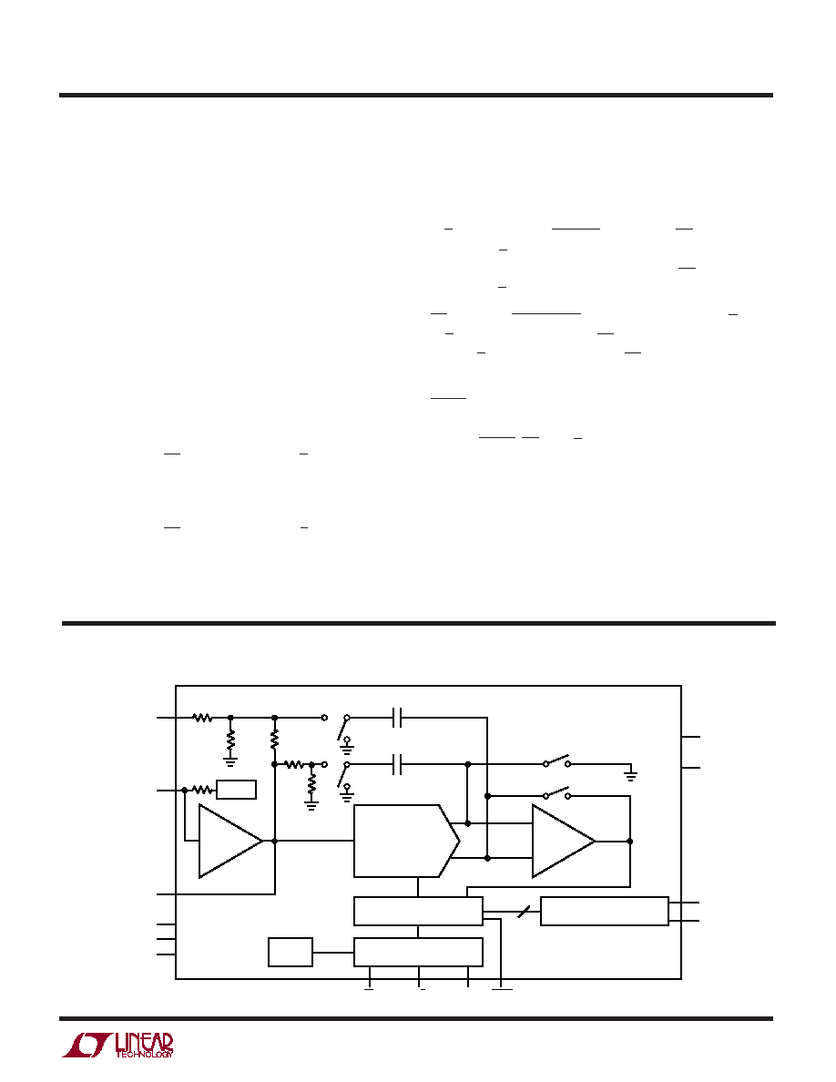
UU
U
PI FU CTIO S
16-BIT CAPACITIVE DAC
COMP
REF BUF
1.64x
2.5V REF
CAP
(4.096V)
CSAMPLE
D15
D0
BUSY
CONTROL LOGIC
R/C
BYTE
INTERNAL
CLOCK
CS
ZEROING SWITCHES
VDIG
VANA
VIN
REF
AGND1
AGND2
DGND
16
1606 BD
+
–
SUCCESSIVE APPROXIMATION
REGISTER
OUTPUT LATCHES
4k
7.35k
2.5k
9k
UU
W
FU CTIO AL BLOCK DIAGRA
相关PDF资料 |
PDF描述 |
|---|---|
| VI-BN3-MW-F3 | CONVERTER MOD DC/DC 24V 100W |
| D38999/20WF32PA | CONN RCPT 32POS WALL MNT W/PINS |
| ADM213EARS | IC TX/RX RS-232 5V 0.1UF 28SSOP |
| MS3108E20-3S | CONN PLUG 3POS RT ANG W/SCKT |
| ADM211EARS | IC TX/RX RS-232 5V 0.1UF 28SSOP |
相关代理商/技术参数 |
参数描述 |
|---|---|
| LTC1606AISW#PBF | 功能描述:IC A/D CONV 16BIT SAMPLNG 28SOIC RoHS:是 类别:集成电路 (IC) >> 数据采集 - 模数转换器 系列:- 标准包装:1 系列:- 位数:14 采样率(每秒):83k 数据接口:串行,并联 转换器数目:1 功率耗散(最大):95mW 电压电源:双 ± 工作温度:0°C ~ 70°C 安装类型:通孔 封装/外壳:28-DIP(0.600",15.24mm) 供应商设备封装:28-PDIP 包装:管件 输入数目和类型:1 个单端,双极 |
| LTC1606AISW#TR | 功能描述:IC ADC 16BIT 5V SAMPLING 28SOIC RoHS:否 类别:集成电路 (IC) >> 数据采集 - 模数转换器 系列:- 标准包装:1 系列:- 位数:14 采样率(每秒):83k 数据接口:串行,并联 转换器数目:1 功率耗散(最大):95mW 电压电源:双 ± 工作温度:0°C ~ 70°C 安装类型:通孔 封装/外壳:28-DIP(0.600",15.24mm) 供应商设备封装:28-PDIP 包装:管件 输入数目和类型:1 个单端,双极 |
| LTC1606AISW#TRPBF | 功能描述:IC A/D CONV 16BIT SAMPLNG 28SOIC RoHS:是 类别:集成电路 (IC) >> 数据采集 - 模数转换器 系列:- 产品培训模块:Lead (SnPb) Finish for COTS Obsolescence Mitigation Program 标准包装:2,500 系列:- 位数:12 采样率(每秒):3M 数据接口:- 转换器数目:- 功率耗散(最大):- 电压电源:- 工作温度:- 安装类型:表面贴装 封装/外壳:SOT-23-6 供应商设备封装:SOT-23-6 包装:带卷 (TR) 输入数目和类型:- |
| LTC1606CG | 功能描述:IC ADC 16BIT 5V SAMPLING 28SSOP RoHS:否 类别:集成电路 (IC) >> 数据采集 - 模数转换器 系列:- 标准包装:1 系列:- 位数:14 采样率(每秒):83k 数据接口:串行,并联 转换器数目:1 功率耗散(最大):95mW 电压电源:双 ± 工作温度:0°C ~ 70°C 安装类型:通孔 封装/外壳:28-DIP(0.600",15.24mm) 供应商设备封装:28-PDIP 包装:管件 输入数目和类型:1 个单端,双极 |
| LTC1606CG#PBF | 功能描述:IC ADC 16BIT SMPL 250KSPS 28SSOP RoHS:是 类别:集成电路 (IC) >> 数据采集 - 模数转换器 系列:- 标准包装:1 系列:- 位数:14 采样率(每秒):83k 数据接口:串行,并联 转换器数目:1 功率耗散(最大):95mW 电压电源:双 ± 工作温度:0°C ~ 70°C 安装类型:通孔 封装/外壳:28-DIP(0.600",15.24mm) 供应商设备封装:28-PDIP 包装:管件 输入数目和类型:1 个单端,双极 |
发布紧急采购,3分钟左右您将得到回复。