- 您现在的位置:买卖IC网 > PDF目录10117 > LTC1609AISW#TR (Linear Technology)IC ADC SRL 16BIT 200KSPS 20-SOIC PDF资料下载
参数资料
| 型号: | LTC1609AISW#TR |
| 厂商: | Linear Technology |
| 文件页数: | 11/24页 |
| 文件大小: | 0K |
| 描述: | IC ADC SRL 16BIT 200KSPS 20-SOIC |
| 标准包装: | 2,000 |
| 位数: | 16 |
| 采样率(每秒): | 200k |
| 数据接口: | 串行 |
| 转换器数目: | 1 |
| 功率耗散(最大): | 100mW |
| 电压电源: | 模拟和数字 |
| 工作温度: | -40°C ~ 85°C |
| 安装类型: | 表面贴装 |
| 封装/外壳: | 20-SOIC(0.295",7.50mm 宽) |
| 供应商设备封装: | 20-SOIC |
| 包装: | 带卷 (TR) |
| 输入数目和类型: | 3 个单端,单极;3 个单端,双极 |
| 其它名称: | LTC1609AISWTR |
19
LTC1609
1609fa
Output Data Format
The SB/BTC pin controls the format of the serial digital
output word. With the pin tied high the format is straight
binary. With the pin tied low the data format is two’s
complement. See Table 1c.
Board Layout, Power Supplies and Decoupling
Wire wrap boards are not recommended for high resolu-
tion or high speed A/D converters. To obtain the best
performance from the LTC1609, a printed circuit board is
required. Layout for the printed circuit board should
ensure the digital and analog signal lines are separated as
much as possible. In particular, care should be taken not
to run any digital track alongside an analog signal track or
underneath the ADC. The analog input should be screened
by AGND.
APPLICATIO S I FOR ATIO
WU
UU
B15
0
123456789
10
11
12
13
14
15
16
17
18
19
20
21
22
23
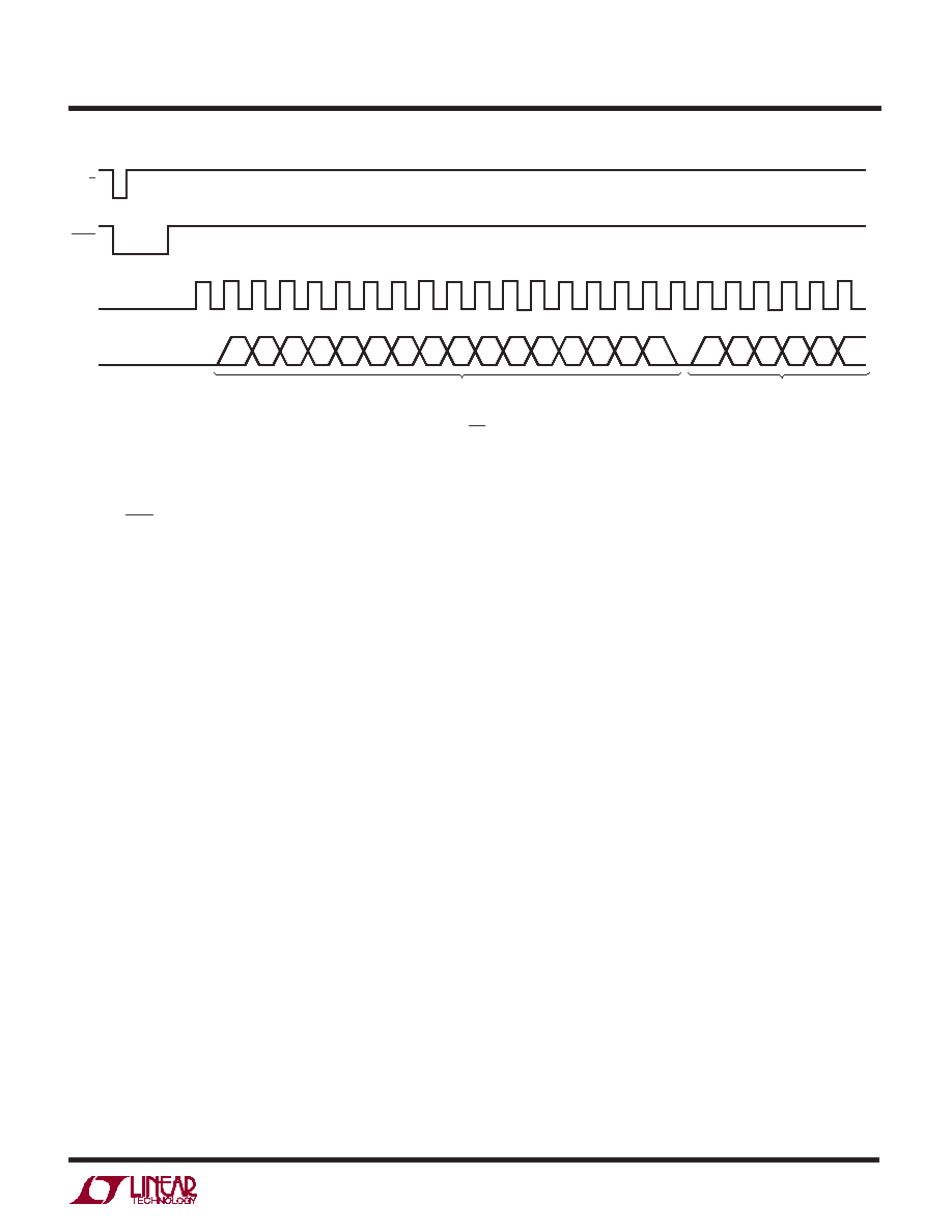
R/C
BUSY
DCLK
DATA
OUT
B14
B13
B12
B11
B10
B9
B8
B7
B6
B5
B4
B3
DEVICE DATA #1
DEVICE DATA #2
B2
B1
B0
NULL
BIT
B14
B13
B12
B11
B10
1609 F14
B15
Figure 14. Data Output from Cascading Two (CS = Low, TAG (#2) = Low) LTC1609s Together
Pay particular attention to the design of the analog and
digital ground planes. Placing the bypass capacitor as
close as possible to the VDIG and VANA pins, the REF pin
and reference buffer output is very important. Low imped-
ance common returns for these bypass capacitors are
essential to low noise operation of the ADC, and the foil
width for these tracks should be as wide as possible. Also,
since any potential difference in grounds between the
signal source and ADC appears as an error voltage in
series with the input signal, attention should be paid to
reducing the ground circuit impedance as much as pos-
sible. The digital output latches and the onboard sampling
clock have been placed on the digital ground plane. The
two ground planes are tied together at the power supply
ground connection.
A “postage stamp” (1.6in
× 1.5in) evaluation board is
available and allows fast in-situ evaluation of the LTC1609.
See Figures 15a through 15d, inclusive.
相关PDF资料 |
PDF描述 |
|---|---|
| SP487ET-L | IC DVR RS485/RS422 QUAD 16SOIC |
| LT1328CMS8#TR | IC RECEIVER IR 4MBPS IRDA 8MSOP |
| ADM1486AR-REEL7 | IC TXRX RS-485 PRO-BUS 5V 8SOIC |
| MS3101A22-10P | CONN RCPT 4POS FREE HNG W/PINS |
| AD7711AR-REEL7 | IC ADC 24BIT RTD I SOURCE 24SOIC |
相关代理商/技术参数 |
参数描述 |
|---|---|
| LTC1609CG | 功能描述:IC CONV A/D 16BIT 200KSPS 28SSOP RoHS:否 类别:集成电路 (IC) >> 数据采集 - 模数转换器 系列:- 标准包装:1,000 系列:- 位数:12 采样率(每秒):300k 数据接口:并联 转换器数目:1 功率耗散(最大):75mW 电压电源:单电源 工作温度:0°C ~ 70°C 安装类型:表面贴装 封装/外壳:24-SOIC(0.295",7.50mm 宽) 供应商设备封装:24-SOIC 包装:带卷 (TR) 输入数目和类型:1 个单端,单极;1 个单端,双极 |
| LTC1609CG#PBF | 功能描述:IC CONV A/D 16BIT 200KSPS 28SSOP RoHS:是 类别:集成电路 (IC) >> 数据采集 - 模数转换器 系列:- 标准包装:1,000 系列:- 位数:12 采样率(每秒):300k 数据接口:并联 转换器数目:1 功率耗散(最大):75mW 电压电源:单电源 工作温度:0°C ~ 70°C 安装类型:表面贴装 封装/外壳:24-SOIC(0.295",7.50mm 宽) 供应商设备封装:24-SOIC 包装:带卷 (TR) 输入数目和类型:1 个单端,单极;1 个单端,双极 |
| LTC1609CG#TR | 功能描述:IC CONV A/D 16BIT 200KSPS 28SSOP RoHS:否 类别:集成电路 (IC) >> 数据采集 - 模数转换器 系列:- 标准包装:1,000 系列:- 位数:12 采样率(每秒):300k 数据接口:并联 转换器数目:1 功率耗散(最大):75mW 电压电源:单电源 工作温度:0°C ~ 70°C 安装类型:表面贴装 封装/外壳:24-SOIC(0.295",7.50mm 宽) 供应商设备封装:24-SOIC 包装:带卷 (TR) 输入数目和类型:1 个单端,单极;1 个单端,双极 |
| LTC1609CG#TRPBF | 功能描述:IC CONV A/D 16BIT 200KSPS 28SSOP RoHS:是 类别:集成电路 (IC) >> 数据采集 - 模数转换器 系列:- 标准包装:1,000 系列:- 位数:12 采样率(每秒):300k 数据接口:并联 转换器数目:1 功率耗散(最大):75mW 电压电源:单电源 工作温度:0°C ~ 70°C 安装类型:表面贴装 封装/外壳:24-SOIC(0.295",7.50mm 宽) 供应商设备封装:24-SOIC 包装:带卷 (TR) 输入数目和类型:1 个单端,单极;1 个单端,双极 |
| LTC1609CGPBF | 制造商:Linear Technology 功能描述:ADC SAR 200ksps 16-Bit Serial SSOP28 |
发布紧急采购,3分钟左右您将得到回复。