参数资料
| 型号: | LTC1654IGN#TR |
| 厂商: | Linear Technology |
| 文件页数: | 13/16页 |
| 文件大小: | 0K |
| 描述: | IC DAC 14BIT DUAL R-R 16SSOP |
| 标准包装: | 2,500 |
| 设置时间: | 3µs |
| 位数: | 14 |
| 数据接口: | 串行 |
| 转换器数目: | 2 |
| 电压电源: | 单电源 |
| 功率耗散(最大): | 750µW |
| 工作温度: | -40°C ~ 85°C |
| 安装类型: | 表面贴装 |
| 封装/外壳: | 16-SSOP(0.154",3.90mm 宽) |
| 供应商设备封装: | 16-SSOP |
| 包装: | 带卷 (TR) |
| 输出数目和类型: | 2 电压,单极;2 电压,双极 |
| 采样率(每秒): | 900k |
6
LTC1654
1654fb
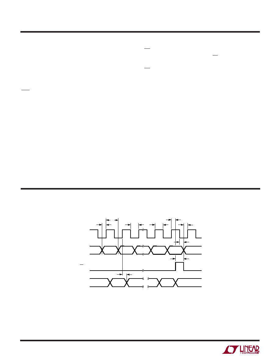
CS/LD (Pin 5): The TTL Level Input for the Serial Interface
Enable and Load Control. When CS/LD is low, the SCK
signal is enabled, so the data can be clocked in. When
CS/LD is pulled high, the control/address bits are
decoded.
DGND/AGND (Pins 6, 12): Digital and Analog Grounds.
SDO (Pin 7): The output of the shift register that becomes
valid on the rising edge of the serial clock.
VOUT A/B (Pins 9, 15): The Buffered DAC Outputs.
REFHI A/B (Pins 10, 14): The Reference High Inputs of the
LTC1654. There is a gain of 1 from this pin to the output
in a gain of 1 configuration. In a gain of 1/2 configuration,
there is a gain of 1/2 from this pin to VOUT.
REFLO A/B (Pins 11, 13): The Reference Low Inputs of the
LTC1654. These inputs can swing up to VCC – 1.5V.
VCC (Pin 16): The Positive Supply Input. 2.7V ≤ VCC ≤ 5.5V.
Requires a 0.1
F bypass capacitor to ground.
X1/X1/2 B, X1/X1/2 A (Pins 1, 8): The Gain of 1 or Gain of
1/2 Pin. When this pin is tied to VOUT, the output range will
be REFLO to (REFLO + REFHI)/2 (0V to REFHI/2 when
REFLO = 0V). When this pin is tied to REFLO, the output
range will be REFLO to REFHI (0V to REFHI when REFLO
= 0V). These pins should not be left floating.
CLR (Pin 2): The Asynchronous Clear Input.
SCK (Pin 3): The TTL Level Input for the Serial Interface
Clock.
SDI (Pin 4): The TTL Level Input for the Serial Interface
Data. Data on the SDI pin is latched into the shift register
on the rising edge of the serial clock. The LTC1654 allows
either a 24-bit or 32-bit word. When a 24-bit word is used,
the first 8 bits are control and address followed by 16 data
bits. The last two of the 16 data bits are don’t cares. When
a 32-bit word (required for daisy-chain operation) is used,
the first 8-bits are don’t cares and the following 24-bits are
as above.
1654 TD01
t1
t4
t3
t5
B0
C3
X
CURRENT WORD
XX
X
XX
SCK
CS/LD
SDI
SDO
t2
t8
t6
t7
t9
(PREVIOUS
WORD)
TI I G DIAGRA S
U
W
UU
U
PI FU CTIO S
相关PDF资料 |
PDF描述 |
|---|---|
| LTC1655LIS8#TRPBF | IC DAC 16BIT R-R MICROPWR 8SOIC |
| LTC1657LIN | IC DAC 16BIT R-R MICROPWR 28DIP |
| LTC1658IMS8#TR | IC DAC 14BIT R-R MICROPWR 8MSOP |
| LTC1659IMS8#TRPBF | IC DAC 12BIT R-R 8-MSOP |
| LTC1660IN | IC D/A CONV 10BIT OCTAL 16-DIP |
相关代理商/技术参数 |
参数描述 |
|---|---|
| LTC1655CN8 | 功能描述:IC D/A CONV 16BIT R-R 8-DIP RoHS:否 类别:集成电路 (IC) >> 数据采集 - 数模转换器 系列:- 标准包装:47 系列:- 设置时间:2µs 位数:14 数据接口:并联 转换器数目:1 电压电源:单电源 功率耗散(最大):55µW 工作温度:-40°C ~ 85°C 安装类型:表面贴装 封装/外壳:28-SSOP(0.209",5.30mm 宽) 供应商设备封装:28-SSOP 包装:管件 输出数目和类型:1 电流,单极;1 电流,双极 采样率(每秒):* |
| LTC1655CN8#PBF | 功能描述:IC D/A CONV 16BIT R-R 8-DIP RoHS:是 类别:集成电路 (IC) >> 数据采集 - 数模转换器 系列:- 产品培训模块:Lead (SnPb) Finish for COTS Obsolescence Mitigation Program 标准包装:50 系列:- 设置时间:4µs 位数:12 数据接口:串行 转换器数目:2 电压电源:单电源 功率耗散(最大):- 工作温度:-40°C ~ 85°C 安装类型:表面贴装 封装/外壳:8-TSSOP,8-MSOP(0.118",3.00mm 宽) 供应商设备封装:8-uMAX 包装:管件 输出数目和类型:2 电压,单极 采样率(每秒):* 产品目录页面:1398 (CN2011-ZH PDF) |
| LTC1655CS8 | 功能描述:IC D/A CONV 16BIT R-R 8-SOIC RoHS:否 类别:集成电路 (IC) >> 数据采集 - 数模转换器 系列:- 标准包装:47 系列:- 设置时间:2µs 位数:14 数据接口:并联 转换器数目:1 电压电源:单电源 功率耗散(最大):55µW 工作温度:-40°C ~ 85°C 安装类型:表面贴装 封装/外壳:28-SSOP(0.209",5.30mm 宽) 供应商设备封装:28-SSOP 包装:管件 输出数目和类型:1 电流,单极;1 电流,双极 采样率(每秒):* |
| LTC1655CS8#PBF | 功能描述:IC D/A CONV 16BIT R-R 8-SOIC RoHS:是 类别:集成电路 (IC) >> 数据采集 - 数模转换器 系列:- 产品培训模块:Lead (SnPb) Finish for COTS Obsolescence Mitigation Program 标准包装:50 系列:- 设置时间:4µs 位数:12 数据接口:串行 转换器数目:2 电压电源:单电源 功率耗散(最大):- 工作温度:-40°C ~ 85°C 安装类型:表面贴装 封装/外壳:8-TSSOP,8-MSOP(0.118",3.00mm 宽) 供应商设备封装:8-uMAX 包装:管件 输出数目和类型:2 电压,单极 采样率(每秒):* 产品目录页面:1398 (CN2011-ZH PDF) |
| LTC1655CS8#PBF | 制造商:Linear Technology 功能描述:D/A Converter (D-A) IC 制造商:Linear Technology 功能描述:IC, DAC, 16BIT, 750KSPS, SOIC-8 |
发布紧急采购,3分钟左右您将得到回复。