参数资料
| 型号: | LTC1660CGN |
| 厂商: | Linear Technology |
| 文件页数: | 13/18页 |
| 文件大小: | 0K |
| 描述: | IC D/A CONV 10BIT OCTAL 16-SSOP |
| 标准包装: | 100 |
| 设置时间: | 30µs |
| 位数: | 10 |
| 数据接口: | 串行 |
| 转换器数目: | 8 |
| 电压电源: | 单电源 |
| 功率耗散(最大): | 1mW |
| 工作温度: | 0°C ~ 70°C |
| 安装类型: | 表面贴装 |
| 封装/外壳: | 16-SSOP(0.154",3.90mm 宽) |
| 供应商设备封装: | 16-SSOP |
| 包装: | 管件 |
| 输出数目和类型: | 8 电压,单极;8 电压,双极 |
| 采样率(每秒): | * |
LTC1665/LTC1660
4
166560fa
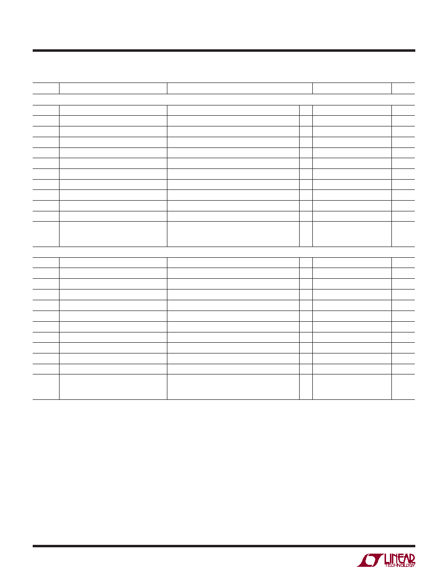
TIMING CHARACTERISTICS The l denotes specifications which apply over the full operating temperature
range, otherwise specifications are at TA = 25°C. (See Figure 1)
SYMBOL
PARAMETER
CONDITIONS
MIN
TYP
MAX
UNITS
VCC = 4.5V to 5.5V
t1
DIN Valid to SCK Setup
l
40
ns
t2
DIN Valid to SCK Hold
l
0ns
t3
SCK High Time
(Note 6)
l
30
ns
t4
SCK Low Time
(Note 6)
l
30
ns
t5
CS/LD Pulse Width
(Note 6)
l
80
ns
t6
LSB SCK High to CS/LD High
(Note 6)
l
30
ns
t7
CS/LD Low to SCK High
(Note 6)
l
80
ns
t8
DOUT Propagation Delay
CLOAD = 15pF (Note 6)
l
580
ns
t9
SCK Low to CS/LD Low
(Note 6)
l
20
ns
t10
CLR Pulse Width
(Note 6)
l
100
ns
t11
CS/LD High to SCK Positive Edge
(Note 6)
l
30
ns
SCK Frequency
Continuous Square Wave (Note 6)
Continuous 23% Duty Cycle Pulse (Note 6)
Gated Square Wave (Note 6)
l
5.00
7.69
16.7
MHz
VCC = 2.7V to 5.5V
t1
DIN Valid to SCK Setup
(Note 6)
l
60
ns
t2
DIN Valid to SCK Hold
(Note 6)
l
0ns
t3
SCK High Time
(Note 6)
l
50
ns
t4
SCK Low Time
(Note 6)
l
50
ns
t5
CS/LD Pulse Width
(Note 6)
l
100
ns
t6
LSB SCK High to CS/LD High
(Note 6)
l
50
ns
t7
CS/LD Low to SCK High
(Note 6)
l
100
ns
t8
DOUT Propagation Delay
CLOAD = 15pF (Note 6)
l
5
150
ns
t9
SCK Low to CS/LD Low
(Note 6)
l
30
ns
t10
CLR Pulse Width
(Note 6)
l
120
ns
t11
CS/LD High to SCK Positive Edge
(Note 6)
l
30
ns
SCK Frequency
Continuous Square Wave (Note 6)
Continuous 28% Duty Cycle Pulse
Gated Square Wave
l
3.85
5.55
10
MHz
Note 1: Stresses beyond those listed under Absolute Maximum Ratings
may cause permanent damage to the device. Exposure to any Absolute
Maximum Rating condition for extended periods may affect device
reliability and lifetime.
Note 2: Nonlinearity and monotonicity are defined from code 4 to code
255 for the LTC1665 and from code 20 to code 1023 for the LTC1660.
See Applications Information.
Note 3: Digital inputs at 0V or VCC.
Note 4: Load is 10kΩ in parallel with 100pF.
Note 5: VCC = VREF = 5V. DAC switched between 0.1VFS and 0.9VFS,
i.e., codes 26 and 230 for the LTC1665 or codes 102 and 922 for the
LTC1660.
Note 6: Guaranteed by design and not production tested.
Note 7: Measured at code 4 for the LTC1665 and code 20 for the
LTC1660.
相关PDF资料 |
PDF描述 |
|---|---|
| LTC1450LCG | IC D/A CONV 12BIT R-R PAR 24SSOP |
| V375A36H500BG3 | CONVERTER MOD DC/DC 36V 500W |
| LTC2607CDE#TRPBF | IC DAC 16BIT R-R I2C 12-DFN |
| AD5453WBCPZ-RL | IC DAC 14BIT MULT 8LFCSP |
| LTC2624CGN#PBF | IC DAC 12BIT QUAD R-R OUT 16SSOP |
相关代理商/技术参数 |
参数描述 |
|---|---|
| LTC1660CGN#PBF | 功能描述:IC D/A CONV 10BIT OCTAL 16-SSOP RoHS:是 类别:集成电路 (IC) >> 数据采集 - 数模转换器 系列:- 产品培训模块:Lead (SnPb) Finish for COTS Obsolescence Mitigation Program 标准包装:50 系列:- 设置时间:4µs 位数:12 数据接口:串行 转换器数目:2 电压电源:单电源 功率耗散(最大):- 工作温度:-40°C ~ 85°C 安装类型:表面贴装 封装/外壳:8-TSSOP,8-MSOP(0.118",3.00mm 宽) 供应商设备封装:8-uMAX 包装:管件 输出数目和类型:2 电压,单极 采样率(每秒):* 产品目录页面:1398 (CN2011-ZH PDF) |
| LTC1660CGN#PBF | 制造商:Linear Technology 功能描述:IC D/A CONVERTER OCTAL 10-BIT CMOS |
| LTC1660CGN#TR | 功能描述:IC DAC 10BIT OCTAL MCRPWR 16SSOP RoHS:否 类别:集成电路 (IC) >> 数据采集 - 数模转换器 系列:- 标准包装:47 系列:- 设置时间:2µs 位数:14 数据接口:并联 转换器数目:1 电压电源:单电源 功率耗散(最大):55µW 工作温度:-40°C ~ 85°C 安装类型:表面贴装 封装/外壳:28-SSOP(0.209",5.30mm 宽) 供应商设备封装:28-SSOP 包装:管件 输出数目和类型:1 电流,单极;1 电流,双极 采样率(每秒):* |
| LTC1660CGN#TRPBF | 功能描述:IC D/A CONV 10BIT OCTAL 16-SSOP RoHS:是 类别:集成电路 (IC) >> 数据采集 - 数模转换器 系列:- 标准包装:47 系列:- 设置时间:2µs 位数:14 数据接口:并联 转换器数目:1 电压电源:单电源 功率耗散(最大):55µW 工作温度:-40°C ~ 85°C 安装类型:表面贴装 封装/外壳:28-SSOP(0.209",5.30mm 宽) 供应商设备封装:28-SSOP 包装:管件 输出数目和类型:1 电流,单极;1 电流,双极 采样率(每秒):* |
| LTC1660CGNPBF | 制造商:Linear Technology 功能描述:Micropower Octal 10-Bit DAC 1uA SSOP16 |
发布紧急采购,3分钟左右您将得到回复。