- 您现在的位置:买卖IC网 > PDF目录8746 > LTC1663IMS8#TR (Linear Technology)IC DAC 10BIT R-R MICROPWR 8MSOP PDF资料下载
参数资料
| 型号: | LTC1663IMS8#TR |
| 厂商: | Linear Technology |
| 文件页数: | 12/12页 |
| 文件大小: | 0K |
| 描述: | IC DAC 10BIT R-R MICROPWR 8MSOP |
| 标准包装: | 2,500 |
| 设置时间: | 30µs |
| 位数: | 10 |
| 数据接口: | 串行 |
| 转换器数目: | 1 |
| 电压电源: | 单电源 |
| 功率耗散(最大): | 630µW |
| 工作温度: | -40°C ~ 85°C |
| 安装类型: | 表面贴装 |
| 封装/外壳: | 8-TSSOP,8-MSOP(0.118",3.00mm 宽) |
| 供应商设备封装: | 8-MSOP |
| 包装: | 带卷 (TR) |
| 输出数目和类型: | 1 电压,单极 |
| 采样率(每秒): | * |
LTC1663
9
1663fd
APPLICATIONS INFORMATION
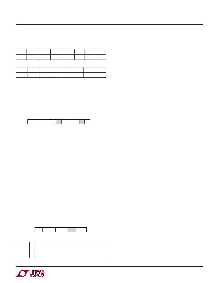
Data Bytes
Least Signicant Data Byte
76
5
4
3
2
1
0
D7
D6
D5
D4
D3
D2
D1
D0
Most Signicant Data Byte
7
6
54
32
1
0
X
XX
D9
D8
X = Don’t care
Send Byte Protocol
The Send Byte protocol used on the LTC1663 is actually a
subset of the Write Word protocol described previously.
The Send Byte protocol can only be used to send the
command byte information to the LTC1663.
Command Byte
A
Slave Address
A
Wr
P
S
81
1
71
1
1663 TA04
1
S = Start Condition, Wr = Write Bit, A = Acknowledge, P = Stop Condition
The Send Byte protocol is also used whenever the Write
Word protocol is interrupted for any reason. Reception of
a START or STOP condition after the Acknowledge of the
command byte, but before the Acknowledge of the last
data byte, will cause both data bytes to be ignored and
the command byte to be accepted.
Reception of a START or STOP condition before the Ac-
knowledge of the command byte will cause the interrupted
command byte to be ignored.
SYNC Address/Quick Command
In addition to the slave address, the LTC1663 has an address
that can be shared by other devices so that they may be
updated synchronously. The address is called to the SYNC
address and uses the quick command protocol.
The SYNC Address is 1111 110
Ack
Stop
Start
1111 110
SY/CLR
11
71
1663 TA05
1
SYNC Address
SY/CLR
1
0
Update output latches on rising edge of SCL during
Acknowledge of SYNC Address
Clear all internal latches on rising edge of SCL during
Acknowledge of SYNC Address
The SY/CLR bit set high only has meaning when the “SY”
bit of the command byte was previously set HIGH. On
the otherhand, the SY/CLR bit set LOW will always clear
the part, independent of the state of the “SY” bit in the
command byte.
Input Threshold
Anticipating the trend toward lower supply voltages,
the SMBus is specied with a VIH of 1.4V and a VIL of
0.6V. While some SMBus parts may violate this stringent
SMBus specication by allowing a higher VIH value for a
correspondingly higher input supply voltage, the LTC1663
meets and maintains the constant SMBus input threshold
specication across the entire supply voltage range of
2.7V to 5.5V. The logic input threshold is designed to be
1V with 50mV of hysteresis.
Voltage Output
The output amplier contained in the LTC1663 can source
or sink up to 5mA. The output stage swings to within a
few millivolts of either supply rail when unloaded and
has an equivalent output resistance of 85Ω when driving
a load to the rails. The output amplier is stable driving
capacitive loads up to 1000pF.
A small resistor placed in series with the output can be
used to achieve stability for any load capacitance greater
than 1000pF. For example, a 0.1μF load can be driven
by the LTC1663 if a 110Ω series resistance is used. The
phase margin of the resulting circuit is 45° and increases
monotonically from this point if larger values of resistance,
capacitance or both are substituted for the values given.
Rail-to-Rail Output Considerations
As in any rail-to-rail device, the output is limited to volt-
ages within the supply range.
If the DAC offset is negative, the output for the lowest
codes limits at 0V as shown in Figure 1b.
Similarly, limiting can occur near full scale when VCC is
used as the reference. If VREF = VCC and the DAC full-scale
error (FSE) is positive, the output for the highest codes
limits at VCC as shown in Figure 1c. No full-scale limiting
can occur if the internal reference is used.
相关PDF资料 |
PDF描述 |
|---|---|
| MC100LVEP11DR2G | IC CLOCK BUFFER 1:2 3GHZ 8-SOIC |
| MC100EP11DR2G | IC CLOCK BUFFER 1:2 3GHZ 8-SOIC |
| VI-B4R-MX | CONVERTER MOD DC/DC 7.5V 75W |
| NB3N551DR2G | IC CLK BUFFER 1:4 180MHZ 8-SOIC |
| VE-JNW-MZ-F4 | CONVERTER MOD DC/DC 5.5V 25W |
相关代理商/技术参数 |
参数描述 |
|---|---|
| LTC1664CGN | 功能描述:IC D/A CONV 10BIT QUAD 16-SSOP RoHS:否 类别:集成电路 (IC) >> 数据采集 - 数模转换器 系列:- 产品培训模块:LTC263x 12-, 10-, and 8-Bit VOUT DAC Family 特色产品:LTC2636 - Octal 12-/10-/8-Bit SPI VOUT DACs with 10ppm/°C Reference 标准包装:91 系列:- 设置时间:4µs 位数:10 数据接口:MICROWIRE?,串行,SPI? 转换器数目:8 电压电源:单电源 功率耗散(最大):2.7mW 工作温度:-40°C ~ 85°C 安装类型:表面贴装 封装/外壳:14-WFDFN 裸露焊盘 供应商设备封装:14-DFN-EP(4x3) 包装:管件 输出数目和类型:8 电压,单极 采样率(每秒):* |
| LTC1664CGN#PBF | 功能描述:IC DAC 10BIT QUAD MICRPWR 16SSOP RoHS:是 类别:集成电路 (IC) >> 数据采集 - 数模转换器 系列:- 产品培训模块:Lead (SnPb) Finish for COTS Obsolescence Mitigation Program 标准包装:50 系列:- 设置时间:4µs 位数:12 数据接口:串行 转换器数目:2 电压电源:单电源 功率耗散(最大):- 工作温度:-40°C ~ 85°C 安装类型:表面贴装 封装/外壳:8-TSSOP,8-MSOP(0.118",3.00mm 宽) 供应商设备封装:8-uMAX 包装:管件 输出数目和类型:2 电压,单极 采样率(每秒):* 产品目录页面:1398 (CN2011-ZH PDF) |
| LTC1664CGN#TR | 功能描述:IC DAC 10BIT QUAD MCRPWR 16SSOP RoHS:否 类别:集成电路 (IC) >> 数据采集 - 数模转换器 系列:- 产品培训模块:LTC263x 12-, 10-, and 8-Bit VOUT DAC Family 特色产品:LTC2636 - Octal 12-/10-/8-Bit SPI VOUT DACs with 10ppm/°C Reference 标准包装:91 系列:- 设置时间:4µs 位数:10 数据接口:MICROWIRE?,串行,SPI? 转换器数目:8 电压电源:单电源 功率耗散(最大):2.7mW 工作温度:-40°C ~ 85°C 安装类型:表面贴装 封装/外壳:14-WFDFN 裸露焊盘 供应商设备封装:14-DFN-EP(4x3) 包装:管件 输出数目和类型:8 电压,单极 采样率(每秒):* |
| LTC1664CGN#TRPBF | 功能描述:IC D/A CONV 10BIT QUAD 16-SSOP RoHS:是 类别:集成电路 (IC) >> 数据采集 - 数模转换器 系列:- 产品培训模块:LTC263x 12-, 10-, and 8-Bit VOUT DAC Family 特色产品:LTC2636 - Octal 12-/10-/8-Bit SPI VOUT DACs with 10ppm/°C Reference 标准包装:91 系列:- 设置时间:4µs 位数:10 数据接口:MICROWIRE?,串行,SPI? 转换器数目:8 电压电源:单电源 功率耗散(最大):2.7mW 工作温度:-40°C ~ 85°C 安装类型:表面贴装 封装/外壳:14-WFDFN 裸露焊盘 供应商设备封装:14-DFN-EP(4x3) 包装:管件 输出数目和类型:8 电压,单极 采样率(每秒):* |
| LTC1664CGNPBF | 制造商:Linear Technology 功能描述:DAC Quad 10-Bit Micropower SSOP16 |
发布紧急采购,3分钟左右您将得到回复。