- 您现在的位置:买卖IC网 > PDF目录14137 > LTC1707CS8#TRPBF (Linear Technology)IC REG BUCK SYNC ADJ 0.6A 8SOIC PDF资料下载
参数资料
| 型号: | LTC1707CS8#TRPBF |
| 厂商: | Linear Technology |
| 文件页数: | 10/16页 |
| 文件大小: | 0K |
| 描述: | IC REG BUCK SYNC ADJ 0.6A 8SOIC |
| 标准包装: | 2,500 |
| 类型: | 降压(降压) |
| 输出类型: | 可调式 |
| 输出数: | 1 |
| 输出电压: | 0.8 V ~ 8.5 V |
| 输入电压: | 2.85 V ~ 8.5 V |
| PWM 型: | 电流模式,混合 |
| 频率 - 开关: | 35kHz ~ 350kHz |
| 电流 - 输出: | 600mA |
| 同步整流器: | 是 |
| 工作温度: | 0°C ~ 70°C |
| 安装类型: | 表面贴装 |
| 封装/外壳: | 8-SOIC(0.154",3.90mm 宽) |
| 包装: | 带卷 (TR) |
| 供应商设备封装: | 8-SOIC |
�� �
�
�LTC1707�
�APPLICATIO� S� I� FOR� ATIO�
�D1� in� Figure� 5� reduces� the� start� delay� but� allows� C� SS� to�
�ramp� up� slowly� providing� the� soft-start� function.� This�
�diode� can� be� deleted� if� soft-start� is� not� needed.�
�Efficiency� Considerations�
�The� efficiency� of� a� switching� regulator� is� equal� to� the�
�output� power� divided� by� the� input� power� times� 100%.� It� is�
�often� useful� to� analyze� individual� losses� to� determine� what�
�is� limiting� the� efficiency� and� which� change� would� produce�
�the� most� improvement.� Efficiency� can� be� expressed� as:�
�Efficiency� =� 100%� –� (L1� +� L2� +� L3� +� ...)�
�where� L1,� L2,� etc.� are� the� individual� losses� as� a� percentage�
�of� input� power.�
�Although� all� dissipative� elements� in� the� circuit� produce�
�losses,� two� main� sources� usually� account� for� most� of� the�
�losses� in� LTC1707� circuits:� V� IN� quiescent� current� and� I� 2� R�
�losses.� The� V� IN� quiescent� current� loss� dominates� the�
�efficiency� loss� at� very� low� load� currents� whereas� the� I� 2� R�
�loss� dominates� the� efficiency� loss� at� medium� to� high� load�
�currents.� In� a� typical� efficiency� plot,� the� efficiency� curve� at�
�very� low� load� currents� can� be� misleading� since� the� actual�
�both� top� and� bottom� MOSFET� R� DS(ON)� and� the� duty�
�cycle� (DC)� as� follows:�
�R� SW� =� (R� DS(ON)TOP� )(DC)� +� (R� DS(ON)BOT� )(1� –� DC)�
�The� R� DS(ON)� for� both� the� top� and� bottom� MOSFETs� can�
�be� obtained� from� the� Typical� Performance� Characteris-�
�tics� curves.� Thus,� to� obtain� I� 2� R� losses,� simply� add� R� SW�
�to� R� L� and� multiply� by� the� square� of� the� average� output�
�current.�
�Other� losses� including� C� IN� and� C� OUT� ESR� dissipative� losses,�
�MOSFET� switching� losses� and� inductor� core� and� copper�
�losses� generally� account� for� less� than� 2%� total� additional�
�loss.�
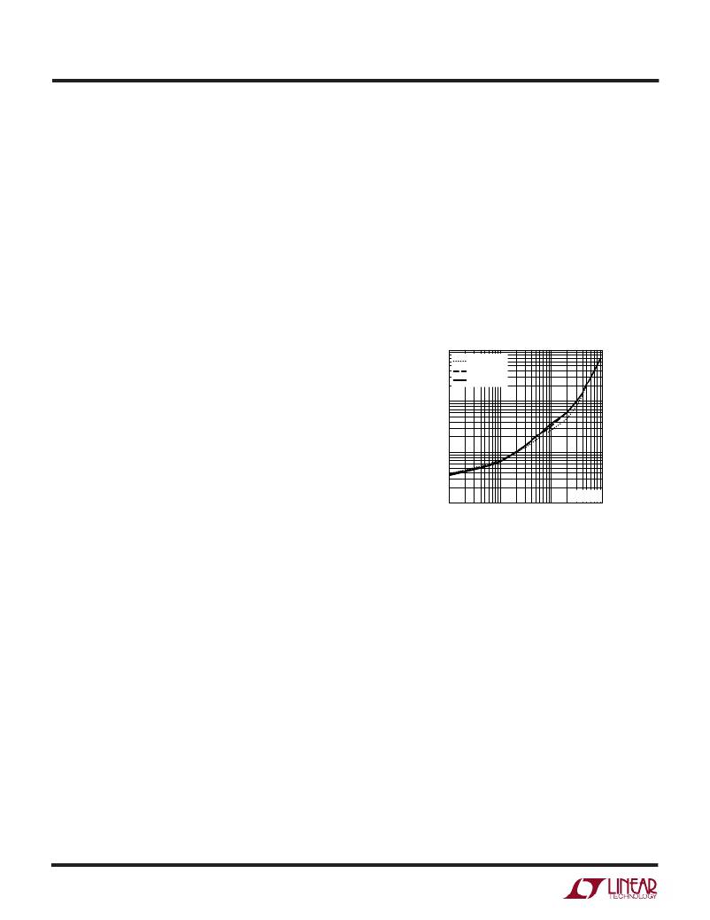
�1�
�V� OUT� =� 1.5V�
�V� OUT� =� 3.3V�
�V� OUT� =� 5V�
�0.1�
�0.01�
�power� lost� is� of� no� consequence� as� illustrated� in� Figure� 6.�
�0.001�
�V� IN� = 6V�
�1.� The� V� IN� quiescent� current� is� due� to� two� components:� the�
�1�
�10� 100�
�LOAD� CURRENT� (mA)�
�1000�
�DC� bias� current� as� given� in� the� electrical� characteristics�
�and� the� internal� main� switch� and� synchronous� switch�
�gate� charge� currents.� The� gate� charge� current� results�
�from� switching� the� gate� capacitance� of� the� internal� power�
�MOSFET� switches.� Each� time� the� gate� is� switched� from�
�high� to� low� or� from� low� to� high,� a� packet� of� charge� dQ�
�moves� from� V� IN� to� ground.� The� resulting� dQ/dt� is� the�
�current� out� of� V� IN� that� is� typically� larger� than� the� DC� bias�
�current.� In� continuous� mode,� I� GATECHG� =� f(Q� T� +� Q� B� )� where�
�Q� T� and� Q� B� are� the� gate� charges� of� the� internal� top� and�
�bottom� switches.� Both� the� DC� bias� and� gate� charge� losses�
�are� proportional� to� V� IN� and� thus� their� effects� will� be� more�
�pronounced� at� higher� supply� voltages.�
�2.� I� 2� R� losses� are� calculated� from� the� resistances� of� the�
�internal� switches� R� SW� and� external� inductor� R� L� .� In�
�continuous� mode� the� average� output� current� flowing�
�through� inductor� L� is� “chopped”� between� the� main�
�switch� and� the� synchronous� switch.� Thus,� the� series�
�resistance� looking� into� SW� pin� from� L� is� a� function� of�
�10�
�1707� F06�
�Figure� 6.� Power� Lost� vs� Load� Current�
�Checking� Transient� Response�
�The� regulator� loop� response� can� be� checked� by� looking� at�
�the� load� transient� response.� Switching� regulators� take�
�several� cycles� to� respond� to� a� step� in� load� current.� When�
�a� load� step� occurs,� V� OUT� immediately� shifts� by� an� amount�
�equal� to� (� ?� I� LOAD� ?� ESR),� where� ESR� is� the� effective� series�
�resistance� of� C� OUT� .� ?� I� LOAD� also� begins� to� charge� or� dis-�
�charge� C� OUT� ,� which� generates� a� feedback� error� signal.� The�
�regulator� loop� then� acts� to� return� V� OUT� to� its� steady-state�
�value.� During� this� recovery� time,� V� OUT� can� be� monitored�
�for� overshoot� or� ringing� that� would� indicate� a� stability�
�problem.� The� internal� compensation� provides� adequate�
�compensation� for� most� applications.� But� if� additional�
�compensation� is� required,� the� I� TH� pin� can� be� used� for�
�external� compensation� as� shown� in� Figure� 7� (the� 47pF�
�capacitor,� C� C2� ,� is� typically� needed� for� noise� decoupling).�
�相关PDF资料 |
PDF描述 |
|---|---|
| LT3483EDC#TRPBF | IC REG INV ADJ 0.2A 8DFN |
| MAX6867UK26D6L+T | IC MPU SUPERVISOR SOT23-5 |
| LT3483ES6#TRPBF | IC REG INV ADJ 0.2A TSOT23-6 |
| MAX6867UK26D5S+T | IC MPU SUPERVISOR SOT23-5 |
| CGS702T250W4L | CAP ALUM 7000UF 250V SCREW |
相关代理商/技术参数 |
参数描述 |
|---|---|
| LTC1707IS8 | 功能描述:IC REG BUCK SYNC ADJ 0.6A 8SOIC RoHS:否 类别:集成电路 (IC) >> PMIC - 稳压器 - DC DC 开关稳压器 系列:- 标准包装:2,500 系列:- 类型:降压(降压) 输出类型:固定 输出数:1 输出电压:1.2V,1.5V,1.8V,2.5V 输入电压:2.7 V ~ 20 V PWM 型:- 频率 - 开关:- 电流 - 输出:50mA 同步整流器:是 工作温度:-40°C ~ 125°C 安装类型:表面贴装 封装/外壳:10-TFSOP,10-MSOP(0.118",3.00mm 宽)裸露焊盘 包装:带卷 (TR) 供应商设备封装:10-MSOP 裸露焊盘 |
| LTC1707IS8#PBF | 功能描述:IC REG BUCK SYNC ADJ 0.6A 8SOIC RoHS:是 类别:集成电路 (IC) >> PMIC - 稳压器 - DC DC 开关稳压器 系列:- 标准包装:2,500 系列:- 类型:降压(降压) 输出类型:固定 输出数:1 输出电压:1.2V,1.5V,1.8V,2.5V 输入电压:2.7 V ~ 20 V PWM 型:- 频率 - 开关:- 电流 - 输出:50mA 同步整流器:是 工作温度:-40°C ~ 125°C 安装类型:表面贴装 封装/外壳:10-TFSOP,10-MSOP(0.118",3.00mm 宽)裸露焊盘 包装:带卷 (TR) 供应商设备封装:10-MSOP 裸露焊盘 |
| LTC1707IS8#TR | 功能描述:IC REG BUCK SYNC ADJ 0.6A 8SOIC RoHS:否 类别:集成电路 (IC) >> PMIC - 稳压器 - DC DC 开关稳压器 系列:- 标准包装:2,500 系列:- 类型:降压(降压) 输出类型:固定 输出数:1 输出电压:1.2V,1.5V,1.8V,2.5V 输入电压:2.7 V ~ 20 V PWM 型:- 频率 - 开关:- 电流 - 输出:50mA 同步整流器:是 工作温度:-40°C ~ 125°C 安装类型:表面贴装 封装/外壳:10-TFSOP,10-MSOP(0.118",3.00mm 宽)裸露焊盘 包装:带卷 (TR) 供应商设备封装:10-MSOP 裸露焊盘 |
| LTC1707IS8#TRPBF | 功能描述:IC REG BUCK SYNC ADJ 0.6A 8SOIC RoHS:是 类别:集成电路 (IC) >> PMIC - 稳压器 - DC DC 开关稳压器 系列:- 标准包装:2,500 系列:- 类型:降压(降压) 输出类型:固定 输出数:1 输出电压:1.2V,1.5V,1.8V,2.5V 输入电压:2.7 V ~ 20 V PWM 型:- 频率 - 开关:- 电流 - 输出:50mA 同步整流器:是 工作温度:-40°C ~ 125°C 安装类型:表面贴装 封装/外壳:10-TFSOP,10-MSOP(0.118",3.00mm 宽)裸露焊盘 包装:带卷 (TR) 供应商设备封装:10-MSOP 裸露焊盘 |
| LTC1707IS8PBF | 制造商:Linear Technology 功能描述:DC-DC Converter Step-Down 2.85-8.5V SO8 |
发布紧急采购,3分钟左右您将得到回复。