- 您现在的位置:买卖IC网 > PDF目录53672 > LTC1731CS8-4.2 (LINEAR TECHNOLOGY CORP) BATTERY CHARGE CONTROLLER, PDSO8 PDF资料下载
参数资料
| 型号: | LTC1731CS8-4.2 |
| 厂商: | LINEAR TECHNOLOGY CORP |
| 元件分类: | 稳压器 |
| 英文描述: | BATTERY CHARGE CONTROLLER, PDSO8 |
| 封装: | 0.150 INCH, PLASTIC, SO-8 |
| 文件页数: | 6/8页 |
| 文件大小: | 99K |
| 代理商: | LTC1731CS8-4.2 |
6
LTC1731
LINEAR TECHNOLOGY CONFIDENTIAL
DRV pin will then be pulled up to VCC and turn off the
external P-channel MOSFET. The internal timer is reset in
the shutdown mode.
Programming Charge Current
The formula for the battery charge current (see Block
Diagram) is:
IBAT = (IPROG)(800/RSENSE)
= (2.457V/RPROG)(800/RSENSE)
where RPROG is the total resistance from the PROG pin to
ground.
For example, if 0.5A charge current is needed, select a
value for RSENSE that will drop 100mV at the maximum
charge current. RSENSE = 0.1V/0.5A = 0.2, then calculate:
RPROG = (2.457V/500mA)(800/0.2) = 19.656k
For best stability over temperature and time, 1% resistors
are recommended. The closest 1% resistor value is 19.6k.
Programming the Timer
The programmable timer is used to terminate the charge.
The length of the timer is programmed by an external
capacitor at the TIMER pin. The total charge time is:
Time = (3 Hours)(CTIMER/0.1F)
The timer starts when the input voltage greater than 4.1V
is applied and the program resistor is connected to ground.
After a time-out occurs, the CHRG output will turn into a
high impedance state to indicate that the charging has
stopped. Connecting the TIMER pin to VCC disables the
timer and also puts the charger into a constant-current
mode. To only disable the timer function, short the TIMER
pin to GND.
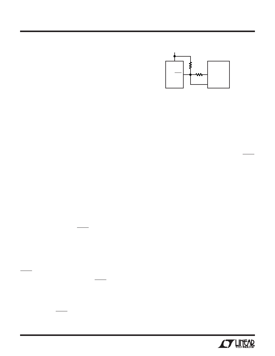
CHRG Status Output Pin
When the charging cycle starts, the CHRG pin is pulled
down to ground by an internal N-channel MOSFET that can
drive an LED. When the battery current drops down to 10%
of the full-scale current (C/10), the N-channel MOSFET is
turned off and a weak 100
A current source to ground is
connected to the CHRG pin. After a time-out occurs, the
pin will go into a high impedance state. By using two
different value pull-up resistors, a microprocessor can
APPLICATIONS INFORMATION
WU
U
detect three states from this pin (charging, C/10 and stop
charging). See Figure 1.
End of Charge (C/10)
The LTC1731 includes a comparator to monitor the charge
current to detect an end-of-charge condition. When the
battery current falls below 10% of full scale, the compara-
tor trips and turns off the N-channel MOSFET at the CHRG
pin and switches in a 100
A current source to ground.
After an internal time delay of 300ms, this state is then
latched. This delay will help prevent false triggering due to
transient currents. The end-of-charge comparator is dis-
abled in trickle charge mode.
Gate Drive
Typically the LTC1731 controls an external P-channel
MOSFET to supply current to the battery. The DRV pin is
internally clamped to 6.5V below VCC. This feature allows
low voltage P-channel MOSFETs with gate to source
breakdown voltage rated at 8V to be used.
An external PNP transistor can also be used as the pass
transistor instead of the P-channel MOSFET. Due to the
low current gain of the current amplifier (CA), a high gain
Darlington PNP transistor is required to avoid too much
charging current error. The gain of the current amplifier is
around 0.6
A/mV. For every 1A of base current, a 1.6mV
of gain error shows up at the inputs of CA. With RPROG =
19.6k (100mV across RSENSE), it represents 1.67% of
error in charging current.
Constant-Current-Only Mode
The LTC1731 can be used as a programmable current
source by forcing the TIMER pin to VCC. This is particu-
larly useful for charging NiMH or NiCd batteries. In the
1k
100k
CHRG
1731 F01
VCC
LTC1731
V +
I/O
PROCESSOR
I/O
2
7
Figure 1. Microprocessor Interface
相关PDF资料 |
PDF描述 |
|---|---|
| LTC1731CS8-8.2 | BATTERY CHARGE CONTROLLER, PDSO8 |
| LTC1735IS8 | SWITCHING CONTROLLER, PDSO8 |
| LTC1735CS8 | SWITCHING CONTROLLER, PDSO8 |
| LTKA00CN8 | SPECIALTY ANALOG CIRCUIT, PDIP8 |
| LTK001MJ8 | SPECIALTY ANALOG CIRCUIT, CDIP8 |
相关代理商/技术参数 |
参数描述 |
|---|---|
| LTC1731EMS8-4.1 | 功能描述:IC CTRLR BATT CHRGR LI-ION 8MSOP RoHS:否 类别:集成电路 (IC) >> PMIC - 电池管理 系列:- 标准包装:61 系列:- 功能:电源管理 电池化学:锂离子(Li-Ion)、锂聚合物(Li-Pol) 电源电压:4.35 V ~ 5.5 V 工作温度:-40°C ~ 85°C 安装类型:表面贴装 封装/外壳:22-WFDFN 裸露焊盘 供应商设备封装:22-DFN(6x3)裸露焊盘 包装:管件 |
| LTC1731EMS8-4.1#PBF | 功能描述:IC CTRLR BATT CHRGR LI-ION 8MSOP RoHS:是 类别:集成电路 (IC) >> PMIC - 电池管理 系列:- 标准包装:61 系列:- 功能:电源管理 电池化学:锂离子(Li-Ion)、锂聚合物(Li-Pol) 电源电压:4.35 V ~ 5.5 V 工作温度:-40°C ~ 85°C 安装类型:表面贴装 封装/外壳:22-WFDFN 裸露焊盘 供应商设备封装:22-DFN(6x3)裸露焊盘 包装:管件 |
| LTC1731EMS8-4.1#TR | 功能描述:IC CTRLR BATT CHRGR LI-ION 8MSOP RoHS:否 类别:集成电路 (IC) >> PMIC - 电池管理 系列:- 标准包装:61 系列:- 功能:电源管理 电池化学:锂离子(Li-Ion)、锂聚合物(Li-Pol) 电源电压:4.35 V ~ 5.5 V 工作温度:-40°C ~ 85°C 安装类型:表面贴装 封装/外壳:22-WFDFN 裸露焊盘 供应商设备封装:22-DFN(6x3)裸露焊盘 包装:管件 |
| LTC1731EMS8-4.1#TRPBF | 功能描述:IC CTRLR BATT CHRGR LI-ION 8MSOP RoHS:是 类别:集成电路 (IC) >> PMIC - 电池管理 系列:- 标准包装:61 系列:- 功能:电源管理 电池化学:锂离子(Li-Ion)、锂聚合物(Li-Pol) 电源电压:4.35 V ~ 5.5 V 工作温度:-40°C ~ 85°C 安装类型:表面贴装 封装/外壳:22-WFDFN 裸露焊盘 供应商设备封装:22-DFN(6x3)裸露焊盘 包装:管件 |
| LTC1731EMS8-4.2 | 功能描述:IC CTRLR BATT CHRGR LI-ION 8MSOP RoHS:否 类别:集成电路 (IC) >> PMIC - 电池管理 系列:- 标准包装:61 系列:- 功能:电源管理 电池化学:锂离子(Li-Ion)、锂聚合物(Li-Pol) 电源电压:4.35 V ~ 5.5 V 工作温度:-40°C ~ 85°C 安装类型:表面贴装 封装/外壳:22-WFDFN 裸露焊盘 供应商设备封装:22-DFN(6x3)裸露焊盘 包装:管件 |
发布紧急采购,3分钟左右您将得到回复。