- 您现在的位置:买卖IC网 > PDF目录10114 > LTC1740CG (Linear Technology)IC ADC 14BIT 6MSPS 36SSOP PDF资料下载
参数资料
| 型号: | LTC1740CG |
| 厂商: | Linear Technology |
| 文件页数: | 6/16页 |
| 文件大小: | 0K |
| 描述: | IC ADC 14BIT 6MSPS 36SSOP |
| 标准包装: | 37 |
| 位数: | 14 |
| 采样率(每秒): | 6M |
| 数据接口: | 并联 |
| 转换器数目: | 1 |
| 功率耗散(最大): | 300mW |
| 电压电源: | 双 ± |
| 工作温度: | 0°C ~ 70°C |
| 安装类型: | 表面贴装 |
| 封装/外壳: | 36-SSOP(0.209",5.30mm 宽) |
| 供应商设备封装: | 36-SSOP |
| 包装: | 管件 |
| 输入数目和类型: | 2 个单端,双极;1 个差分,双极 |
| 产品目录页面: | 1349 (CN2011-ZH PDF) |
14
LTC1740
1740f
As with all fast ADCs, the noise performance of the
LTC1740 is sensitive to clock jitter when high speed inputs
are present. The SNR performance of an ADC when the
performance is limited by jitter is given by:
SNR = – 20log (2
πfINtJ)dB
where fIN is the frequency of an input sine wave and tJ is
the root-mean-square jitter due to the clock, the analog
input and the A/D aperture jitter. To minimize clock jitter,
use a clean clock source such as a crystal oscillator, treat
the clock signals as sensitive analog traces and use
dedicated packages with good supply bypassing for any
clock drivers.
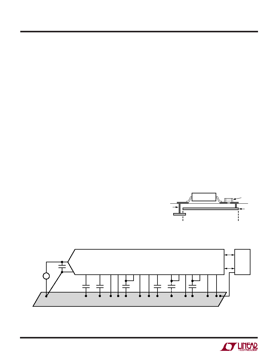
Board Layout
To obtain the best performance from the LTC1740, a
printed circuit board with a ground plane is required.
Layout for the printed circuit board should ensure that
digital and analog signal lines are separated as much as
possible. In particular, care should be taken not to run any
digital track alongside an analog signal track.
An analog ground plane separate from the logic system
ground should be placed under and around the ADC.
Pins 6, 7, 10, 31, 34 (GND), Pins 11, 28 (OGND) and all
other analog grounds should be connected to this ground
plane. In single supply mode, Pins 29, 30 (VSS) should
also be connected to this ground plane. All bypass capaci-
tors for the LTC1740 should also be connected to this
ground plane (Figure 12). The digital system ground
DIGITAL
SYSTEM
–AIN
+AIN
1
2
1000pF
1740 F12
LTC1740
ANALOG GROUND PLANE
1
F
34
32
GND
VDD
33
VDD
31
GND
1
F
19
OVDD
1
F
5
VREF
1
F
3
VCM
11
OGND
10
GND
7
GND
6
GND
1
F
8
VDD
9
VDD
1
F
29
VSS
30
VSS
28
OGND
+
–
ANALOG
INPUT
CIRCUITRY
Figure 12. Power Supply Grounding
should be connected to the analog ground plane at only
one point, near the OGND pin (Pin 28).
The analog ground plane should be as close to the ADC as
possible. Care should be taken to avoid making holes in the
analog ground plane under and around the part. To ac-
complish this, we recommend placing vias for power and
signal traces outside the area containing the part and the
decoupling capacitors (Figure 13).
Supply Bypassing
High quality, low series resistance ceramic 1
F capacitors
should be used at the VDD pins, VCM and VREF. If VSS is
connected to – 5V it should also be bypassed to ground
with 1
F. In single supply operation VSSshouldbeshorted
to the ground plane as close to the part as possible. OVDD
requires a 1
F decoupling capacitor to ground. Surface
mount capacitors such as the AVX 0805ZC105KAT pro-
vide excellent bypassing in a small board space. The traces
connecting the pins and the bypass capacitors must be
kept short and should be made as wide as possible.
APPLICATIO S I FOR ATIO
WU
UU
AVOID BREAKING GROUND PLANE
IN THIS AREA
PLACE NON-GROUND
VIAS AWAY FROM
GROUND PLANE AND
BYPASS CAPACITORS
ANALOG
GROUND
PLANE
BYPASS
CAPACITOR
1740 F13
LTC1740
Figure 13. Cross Section of the LTC1740 Printed Circuit Board
相关PDF资料 |
PDF描述 |
|---|---|
| CS3102A-32-76SY | CONN RCPT 19POS BOX MNT W/SCKT |
| MS3102E22-22SY | CONN RCPT 4POS BOX MNT W/SCKT |
| CS3102A-32-76S | CONN RCPT 19POS BOX MNT W/SCKT |
| IDT72V201L10J8 | IC FIFO SYNC 256X9 10NS 32-PLCC |
| MS27656E21B39S | CONN RCPT 39POS WALL MNT W/SCKT |
相关代理商/技术参数 |
参数描述 |
|---|---|
| LTC1740CG#PBF | 功能描述:IC ADC 14BIT 6MSPS 36SSOP RoHS:是 类别:集成电路 (IC) >> 数据采集 - 模数转换器 系列:- 标准包装:1 系列:- 位数:14 采样率(每秒):83k 数据接口:串行,并联 转换器数目:1 功率耗散(最大):95mW 电压电源:双 ± 工作温度:0°C ~ 70°C 安装类型:通孔 封装/外壳:28-DIP(0.600",15.24mm) 供应商设备封装:28-PDIP 包装:管件 输入数目和类型:1 个单端,双极 |
| LTC1740CG#TR | 功能描述:IC ADC SMPL 14BIT 6MSPS 36-SSOP RoHS:否 类别:集成电路 (IC) >> 数据采集 - 模数转换器 系列:- 标准包装:1,000 系列:- 位数:12 采样率(每秒):300k 数据接口:并联 转换器数目:1 功率耗散(最大):75mW 电压电源:单电源 工作温度:0°C ~ 70°C 安装类型:表面贴装 封装/外壳:24-SOIC(0.295",7.50mm 宽) 供应商设备封装:24-SOIC 包装:带卷 (TR) 输入数目和类型:1 个单端,单极;1 个单端,双极 |
| LTC1740CG#TRPBF | 功能描述:IC ADC 14BIT 6MSPS 36SSOP RoHS:是 类别:集成电路 (IC) >> 数据采集 - 模数转换器 系列:- 标准包装:1,000 系列:- 位数:12 采样率(每秒):300k 数据接口:并联 转换器数目:1 功率耗散(最大):75mW 电压电源:单电源 工作温度:0°C ~ 70°C 安装类型:表面贴装 封装/外壳:24-SOIC(0.295",7.50mm 宽) 供应商设备封装:24-SOIC 包装:带卷 (TR) 输入数目和类型:1 个单端,单极;1 个单端,双极 |
| LTC1740IG | 功能描述:IC ADC SMPL 14BIT 6MSPS 36-SSOP RoHS:否 类别:集成电路 (IC) >> 数据采集 - 模数转换器 系列:- 标准包装:1 系列:- 位数:14 采样率(每秒):83k 数据接口:串行,并联 转换器数目:1 功率耗散(最大):95mW 电压电源:双 ± 工作温度:0°C ~ 70°C 安装类型:通孔 封装/外壳:28-DIP(0.600",15.24mm) 供应商设备封装:28-PDIP 包装:管件 输入数目和类型:1 个单端,双极 |
| LTC1740IG#PBF | 功能描述:IC ADC 14BIT 6MSPS 36SSOP RoHS:是 类别:集成电路 (IC) >> 数据采集 - 模数转换器 系列:- 标准包装:1 系列:- 位数:14 采样率(每秒):83k 数据接口:串行,并联 转换器数目:1 功率耗散(最大):95mW 电压电源:双 ± 工作温度:0°C ~ 70°C 安装类型:通孔 封装/外壳:28-DIP(0.600",15.24mm) 供应商设备封装:28-PDIP 包装:管件 输入数目和类型:1 个单端,双极 |
发布紧急采购,3分钟左右您将得到回复。