参数资料
| 型号: | LTC1740IG#TRPBF |
| 厂商: | Linear Technology |
| 文件页数: | 2/16页 |
| 文件大小: | 0K |
| 描述: | IC ADC 14BIT 6MSPS 36SSOP |
| 标准包装: | 2,000 |
| 位数: | 14 |
| 采样率(每秒): | 6M |
| 数据接口: | 并联 |
| 转换器数目: | 1 |
| 功率耗散(最大): | 300mW |
| 电压电源: | 双 ± |
| 工作温度: | -40°C ~ 85°C |
| 安装类型: | 表面贴装 |
| 封装/外壳: | 36-SSOP(0.209",5.30mm 宽) |
| 供应商设备封装: | 36-SSOP |
| 包装: | 带卷 (TR) |
| 输入数目和类型: | 2 个单端,双极;1 个差分,双极 |
10
LTC1740
1740f
APPLICATIO S I FOR ATIO
WU
UU
reference amplifier drives the VREF pin. If SENSE is tied to
ground, the reference amplifier feedback is connected to
the R1/R2 voltage divider, thus making VREF = 4.500V. If
SENSE is tied to VREF, the reference amplifier feedback is
connected to SENSE thus making VREF = 2.250V. If SENSE
is tied to VDD, the reference amplifier is disconnected from
VREF and VREF can be driven by an external voltage. With
additional resistors between VREF and SENSE, and SENSE
and GND, VREF can be set to any voltage between 2.250V
and 4.5V.
An external reference or a DAC can be used to drive VREF
over a 0V to 5V range (Figures 3a and 3b). The input
impedance of the VREF pin is 1k, so a buffer may be
required for high accuracy. Driving VREF with a DAC is
useful in applications where the peak input signal ampli-
tude may vary. The input span of the ADC can then be
adjusted to match the peak input signal, maximizing the
signal-to-noise ratio.
VOUT
VIN
LT1019A-2.5
5V
1740 F03a
1
F
1
F
VREF
SENSE
5V
VCM
LTC1740
Figure 3a. Using the LT1019-2.5 as an
External Reference; Input Range =
±1.39V
1740 F03b
1
F
1
F
VREF
LTC1740
SENSE
VCM
2.250V
–
+
5k
LTC1450
Figure 3b. Driving VREF with a DAC
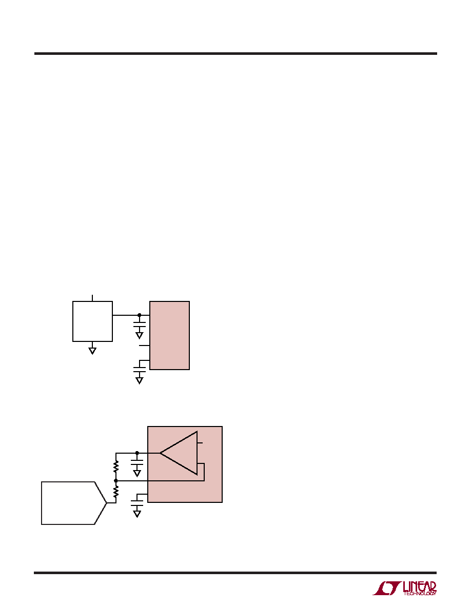
Both the VCM and VREF pins must be bypassed with
capacitors to ground. For best performance, 1
F or larger
ceramic capacitors are recommended. For the case of
external circuitry driving VREF, a smaller capacitor can be
used at VREF so the input range can be changed quickly.
In this case, a 0.2
F or larger ceramic capacitor is
acceptable.
The VCM pin is a low output impedance 2.5V reference that
can be used by external circuitry. For single 5V supply
applications it is convenient to connect AIN– directly to the
VCM pin.
Driving the Analog Inputs
The differential inputs of the LTC1740 are easy to drive.
The inputs may be driven differentially or single-ended
(i. e., the AIN– input is held at a fixed value). The AIN– and
AIN+ inputs are simultaneously sampled and any common
mode signal is reduced by the high common mode rejec-
tion of the sample-and-hold circuit. Any common mode
input value is acceptable as long as the input pins stay
between VDD and VSS. During conversion the analog
inputs are high impedance. At the end of conversion the
inputs draw a small current spike while charging the
sample-and-hold.
For superior dynamic performance in dual supply mode,
the LTC1740 should be operated with the analog inputs
centered at ground, and in single supply mode the inputs
should be centered at 2.5V. For the best dynamic perfor-
mance, the analog inputs can be driven differentially via a
transformer or differential amplifier.
DC Coupling the Input
In many applications the analog input signal can be
directly coupled to the LTC1740 inputs. If the input signal
is centered around ground, such as when dual supply op
amps are used, simply connect AIN– to ground and con-
nect VSS to – 5V (Figure 4). In a single power supply
system with the input signal centered around 2.5V, con-
nect AIN– to VCM and VSS to ground (Figure 5). If the input
signal is not centered around ground or 2.5V, the voltage
for AIN– must be generated externally by a resistor divider
or a voltage reference (Figure 6).
相关PDF资料 |
PDF描述 |
|---|---|
| LTC1741IFW#PBF | IC ADC 12BIT 65MSPS 48-TSSOP |
| LTC1742CFW#TRPBF | IC ADC 14BIT 65MSPS 48-TSSOP |
| LTC1743IFW#PBF | IC ADC 12BIT 50MSPS SMPL 48TSSOP |
| LTC1744IFW#TRPBF | IC ADC 14BIT 50MSPS 48-TSSOP |
| LTC1745CFW#TRPBF | IC ADC 12BIT 25MSPS LN 48TSSOP |
相关代理商/技术参数 |
参数描述 |
|---|---|
| LTC1741CFW | 功能描述:IC ADC 12BIT 65MSPS 48-TSSOP RoHS:否 类别:集成电路 (IC) >> 数据采集 - 模数转换器 系列:- 其它有关文件:TSA1204 View All Specifications 标准包装:1 系列:- 位数:12 采样率(每秒):20M 数据接口:并联 转换器数目:2 功率耗散(最大):155mW 电压电源:模拟和数字 工作温度:-40°C ~ 85°C 安装类型:表面贴装 封装/外壳:48-TQFP 供应商设备封装:48-TQFP(7x7) 包装:Digi-Reel® 输入数目和类型:4 个单端,单极;2 个差分,单极 产品目录页面:1156 (CN2011-ZH PDF) 其它名称:497-5435-6 |
| LTC1741CFW#PBF | 功能描述:IC ADC 12BIT 65MSPS 48-TSSOP RoHS:是 类别:集成电路 (IC) >> 数据采集 - 模数转换器 系列:- 产品培训模块:Lead (SnPb) Finish for COTS Obsolescence Mitigation Program 标准包装:2,500 系列:- 位数:12 采样率(每秒):3M 数据接口:- 转换器数目:- 功率耗散(最大):- 电压电源:- 工作温度:- 安装类型:表面贴装 封装/外壳:SOT-23-6 供应商设备封装:SOT-23-6 包装:带卷 (TR) 输入数目和类型:- |
| LTC1741CFW#TR | 功能描述:IC ADC SMPL 12BIT 65MSPS 48TSSOP RoHS:否 类别:集成电路 (IC) >> 数据采集 - 模数转换器 系列:- 标准包装:1,000 系列:- 位数:12 采样率(每秒):300k 数据接口:并联 转换器数目:1 功率耗散(最大):75mW 电压电源:单电源 工作温度:0°C ~ 70°C 安装类型:表面贴装 封装/外壳:24-SOIC(0.295",7.50mm 宽) 供应商设备封装:24-SOIC 包装:带卷 (TR) 输入数目和类型:1 个单端,单极;1 个单端,双极 |
| LTC1741CFW#TRPBF | 功能描述:IC ADC 12BIT 65MSPS 48-TSSOP RoHS:是 类别:集成电路 (IC) >> 数据采集 - 模数转换器 系列:- 产品培训模块:Lead (SnPb) Finish for COTS Obsolescence Mitigation Program 标准包装:2,500 系列:- 位数:12 采样率(每秒):3M 数据接口:- 转换器数目:- 功率耗散(最大):- 电压电源:- 工作温度:- 安装类型:表面贴装 封装/外壳:SOT-23-6 供应商设备封装:SOT-23-6 包装:带卷 (TR) 输入数目和类型:- |
| LTC1741IFW | 功能描述:IC ADC SMPL 12BIT 65MSPS 48TSSOP RoHS:否 类别:集成电路 (IC) >> 数据采集 - 模数转换器 系列:- 标准包装:1,000 系列:- 位数:12 采样率(每秒):300k 数据接口:并联 转换器数目:1 功率耗散(最大):75mW 电压电源:单电源 工作温度:0°C ~ 70°C 安装类型:表面贴装 封装/外壳:24-SOIC(0.295",7.50mm 宽) 供应商设备封装:24-SOIC 包装:带卷 (TR) 输入数目和类型:1 个单端,单极;1 个单端,双极 |
发布紧急采购,3分钟左右您将得到回复。