参数资料
| 型号: | LTC1741IFW#PBF |
| 厂商: | Linear Technology |
| 文件页数: | 3/20页 |
| 文件大小: | 0K |
| 描述: | IC ADC 12BIT 65MSPS 48-TSSOP |
| 标准包装: | 39 |
| 位数: | 12 |
| 采样率(每秒): | 65M |
| 数据接口: | 并联 |
| 转换器数目: | 1 |
| 功率耗散(最大): | 1.38W |
| 电压电源: | 单电源 |
| 工作温度: | -40°C ~ 85°C |
| 安装类型: | 表面贴装 |
| 封装/外壳: | 48-TFSOP(0.240",6.10mm 宽) |
| 供应商设备封装: | 48-TSSOP |
| 包装: | 管件 |
| 输入数目和类型: | 2 个单端,双极;1 个差分,双极 |
11
LTC1741
1741f
APPLICATIO S I FOR ATIO
WU
UU
CONVERTER OPERATION
The LTC1741 is a CMOS pipelined multistep converter.
The converter has four pipelined ADC stages; a sampled
analog input will result in a digitized value five cycles later,
see the Timing Diagram section. The analog input is
differential for improved common mode noise immunity
and to maximize the input range. Additionally, the differen-
tial input drive will reduce even order harmonics of the
sample-and-hold circuit. The encode input is also
differential for improved common mode noise immunity.
The LTC1741 has two phases of operation, determined by
the state of the differential ENC/ENC input pins. For brev-
ity, the text will refer to ENC greater than ENC as ENC high
and ENC less than ENC as ENC low.
Each pipelined stage shown in Figure 1 contains an ADC,
a reconstruction DAC and an interstage residue amplifier.
In operation, the ADC quantizes the input to the stage and
the quantized value is subtracted from the input by the
DAC to produce a residue. The residue is amplified and
output by the residue amplifier. Successive stages operate
out of phase so that when the odd stages are outputting
their residue, the even stages are acquiring that residue
and visa versa.
When ENC is low, the analog input is sampled differentially
directly onto the input sample-and-hold capacitors, inside
the “Input S/H” shown in the block diagram. At the instant
that ENC transitions from low to high, the sampled input
is held. While ENC is high, the held input voltage is
buffered by the S/H amplifier which drives the first pipelined
ADC stage. The first stage acquires the output of the S/H
during this high phase of ENC. When ENC goes back low,
the first stage produces its residue which is acquired by
the second stage. At the same time, the input S/H goes
back to acquiring the analog input. When ENC goes back
high, the second stage produces its residue which is
acquired by the third stage. An identical process is re-
peated for the third stage, resulting in a third stage residue
that is sent to the fourth stage ADC for final evaluation.
Each ADC stage following the first has additional range to
accommodate flash and amplifier offset errors. Results
from all of the ADC stages are digitally synchronized such
that the results can be properly combined in the correction
logic before being sent to the output buffer.
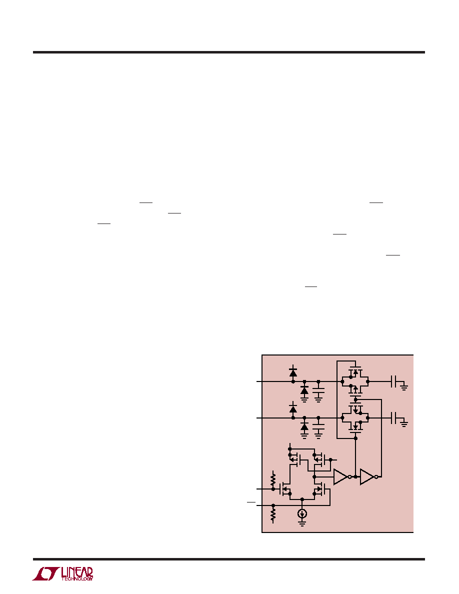
SAMPLE/HOLD OPERATION AND INPUT DRIVE
Sample/Hold Operation
Figure 2 shows an equivalent circuit for the LTC1741
CMOS differential sample-and-hold. The differential ana-
log inputs are sampled directly onto sampling capacitors
(CSAMPLE) through CMOS transmission gates. This direct
capacitor sampling results in lowest possible noise for a
given sampling capacitor size. The capacitors shown
attached to each input (CPARASITIC) are the summation of
all other capacitance associated with each input.
During the sample phase when ENC/ENC is low, the
transmission gate connects the analog inputs to the sam-
pling capacitors and they charge to, and track the differen-
tial input voltage. When ENC/ENC transitions from low to
high the sampled input voltage is held on the sampling
capacitors. During the hold phase when ENC/ENC is high
the sampling capacitors are disconnected from the input
and the held voltage is passed to the ADC core for
processing. As ENC/ENC transitions from high to low the
inputs are reconnected to the sampling capacitors to
acquire a new sample. Since the sampling capacitors still
hold the previous sample, a charging glitch proportional to
the change in voltage between samples will be seen at this
CSAMPLE
4pF
VDD
LTC1741
AIN
+
1741 F02
CSAMPLE
4pF
BIAS
VDD
5V
AIN
–
ENC
2V
6k
2V
6k
CPARASITIC
Figure 2. Equivalent Input Circuit
相关PDF资料 |
PDF描述 |
|---|---|
| LTC1742CFW#TRPBF | IC ADC 14BIT 65MSPS 48-TSSOP |
| LTC1743IFW#PBF | IC ADC 12BIT 50MSPS SMPL 48TSSOP |
| LTC1744IFW#TRPBF | IC ADC 14BIT 50MSPS 48-TSSOP |
| LTC1745CFW#TRPBF | IC ADC 12BIT 25MSPS LN 48TSSOP |
| LTC1746IFW#TRPBF | IC ADC 14BIT 25MSPS LP 48TSSOP |
相关代理商/技术参数 |
参数描述 |
|---|---|
| LTC1742CFW | 功能描述:IC ADC 14BIT 65MSPS 48-TSSOP RoHS:否 类别:集成电路 (IC) >> 数据采集 - 模数转换器 系列:- 产品培训模块:Lead (SnPb) Finish for COTS Obsolescence Mitigation Program 标准包装:2,500 系列:- 位数:12 采样率(每秒):3M 数据接口:- 转换器数目:- 功率耗散(最大):- 电压电源:- 工作温度:- 安装类型:表面贴装 封装/外壳:SOT-23-6 供应商设备封装:SOT-23-6 包装:带卷 (TR) 输入数目和类型:- |
| LTC1742CFW#PBF | 功能描述:IC ADC 14BIT 65MSPS 48-TSSOP RoHS:是 类别:集成电路 (IC) >> 数据采集 - 模数转换器 系列:- 标准包装:1 系列:- 位数:14 采样率(每秒):83k 数据接口:串行,并联 转换器数目:1 功率耗散(最大):95mW 电压电源:双 ± 工作温度:0°C ~ 70°C 安装类型:通孔 封装/外壳:28-DIP(0.600",15.24mm) 供应商设备封装:28-PDIP 包装:管件 输入数目和类型:1 个单端,双极 |
| LTC1742CFW#TR | 功能描述:IC ADC SMPL 14BIT 65MSPS 48TSSOP RoHS:否 类别:集成电路 (IC) >> 数据采集 - 模数转换器 系列:- 标准包装:1 系列:- 位数:14 采样率(每秒):83k 数据接口:串行,并联 转换器数目:1 功率耗散(最大):95mW 电压电源:双 ± 工作温度:0°C ~ 70°C 安装类型:通孔 封装/外壳:28-DIP(0.600",15.24mm) 供应商设备封装:28-PDIP 包装:管件 输入数目和类型:1 个单端,双极 |
| LTC1742CFW#TRPBF | 功能描述:IC ADC 14BIT 65MSPS 48-TSSOP RoHS:是 类别:集成电路 (IC) >> 数据采集 - 模数转换器 系列:- 产品培训模块:Lead (SnPb) Finish for COTS Obsolescence Mitigation Program 标准包装:2,500 系列:- 位数:12 采样率(每秒):3M 数据接口:- 转换器数目:- 功率耗散(最大):- 电压电源:- 工作温度:- 安装类型:表面贴装 封装/外壳:SOT-23-6 供应商设备封装:SOT-23-6 包装:带卷 (TR) 输入数目和类型:- |
| LTC1742IFW | 功能描述:IC ADC SMPL 14BIT 65MSPS 48TSSOP RoHS:否 类别:集成电路 (IC) >> 数据采集 - 模数转换器 系列:- 标准包装:1 系列:- 位数:14 采样率(每秒):83k 数据接口:串行,并联 转换器数目:1 功率耗散(最大):95mW 电压电源:双 ± 工作温度:0°C ~ 70°C 安装类型:通孔 封装/外壳:28-DIP(0.600",15.24mm) 供应商设备封装:28-PDIP 包装:管件 输入数目和类型:1 个单端,双极 |
发布紧急采购,3分钟左右您将得到回复。