参数资料
| 型号: | LTC1748CFW#TRPBF |
| 厂商: | Linear Technology |
| 文件页数: | 5/20页 |
| 文件大小: | 0K |
| 描述: | IC ADC 14BIT 80MSPS 48-TSSOP |
| 标准包装: | 1,800 |
| 位数: | 14 |
| 采样率(每秒): | 80M |
| 数据接口: | 并联 |
| 转换器数目: | 1 |
| 功率耗散(最大): | 1.55W |
| 电压电源: | 单电源 |
| 工作温度: | 0°C ~ 70°C |
| 安装类型: | 表面贴装 |
| 封装/外壳: | 48-TFSOP(0.240",6.10mm 宽) |
| 供应商设备封装: | 48-TSSOP |
| 包装: | 带卷 (TR) |
| 输入数目和类型: | 2 个单端,双极;1 个差分,双极 |
13
LTC1748
1748fa
Input Drive Impedance
As with all high performance, high speed ADCs the dy-
namic performance of the LTC1748 can be influenced by
the input drive circuitry, particularly the second and third
harmonics. Source impedance and input reactance can
influence SFDR. At the falling edge of encode the sample-
and-hold circuit will connect the 4pF sampling capacitor to
the input pin and start the sampling period. The sampling
period ends when encode rises, holding the sampled input
on the sampling capacitor. Ideally the input circuitry
should be fast enough to fully charge the sampling capaci-
tor during the sampling period 1/(2FENCODE); however,
this is not always possible and the incomplete settling may
degrade the SFDR. The sampling glitch has been designed
to be as linear as possible to minimize the effects of
incomplete settling.
For the best performance, it is recomended to have a
source impedence of 100
or less for each input. The S/H
circuit is optimized for a 50
source impedance. If the
source impedance is less than 50
, a series resistor
should be added to increase this impedance to 50
. The
source impedence should be matched for the differential
inputs. Poor matching will result in higher even order
harmonics, especially the second.
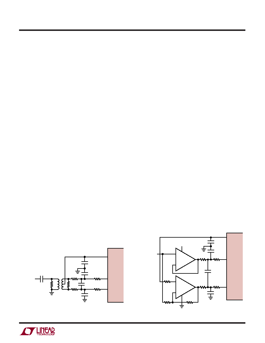
Input Drive Circuits
Figure 3 shows the LTC1748 being driven by an RF
transformer with a center tapped secondary. The second-
ary center tap is DC biased with VCM, setting the ADC input
signal at its optimum DC level. Figure 3 shows a 1:1 turns
ratio transformer. Other turns ratios can be used if the
source impedence seen by the ADC does not exceed
100
for each ADC input. A disadvantage of using a
transformer is the loss of low frequency response. Most
small RF transformers have poor performance at frequen-
cies below 1MHz.
Figure 4 demonstrates the use of operational amplifiers to
convert a single ended input signal into a differential input
signal. The advantage of this method is that it provides low
frequency input response; however, the limited gain band-
width of most op amps will limit the SFDR at high input
frequencies.
The 25
resistors and 12pF capacitors on the analog
inputs serve two purposes: isolating the drive circuitry
from the sample-and-hold charging glitches and limiting
the wideband noise at the converter input. For input
frequencies higher than 100MHz, the capacitors may need
to be decreased to prevent excessive signal loss.
Reference Operation
Figure 5 shows the LTC1748 reference circuitry consisting
of a 2.35V bandgap reference, a difference amplifier and
switching and control circuit. The internal voltage refer-
ence can be configured for two pin selectable input ranges
of 2V(
±1V differential) or 3.2V(±1.6V differential). Tying
the SENSE pin to ground selects the 2V range; tying the
SENSE pin to VDD selects the 3.2V range.
The 2.35V bandgap reference serves two functions: its
output provides a DC bias point for setting the common
APPLICATIO S I FOR ATIO
WU
UU
1:1
25
0.1
F
ANALOG
INPUT
VCM
AIN
+
AIN
–
100
100
12pF
1748 F03
4.7
F
25
25
25
LTC1748
25
5V
SINGLE-ENDED
INPUT
2.35V
±1/2
RANGE
VCM
AIN
+
AIN
–
12pF
1748 F04
4.7
F
25
100
500
500
25
25
LTC1748
–
+
1/2 LT1810
–
+
1/2 LT1810
Figure 4. Differential Drive with Op Amps
Figure 3. Single-Ended to Differential Conversion
Using a Transformer
相关PDF资料 |
PDF描述 |
|---|---|
| LTC1749IFW#PBF | IC ADC 12BIT 80MSPS SMPL 48TSSOP |
| LTC1750IFW#PBF | IC ADC 14BIT 80MSPS SMPL 48TSSOP |
| LTC1799HS5#TRPBF | IC OSC SILICON 33MHZ TSOT23-5 |
| LTC1821ACGW | IC D/A CONV 16BIT PRECISE 36SSOP |
| LTC1851CFW | IC ADC 12BIT 1.25MSPS 48-TSSOP |
相关代理商/技术参数 |
参数描述 |
|---|---|
| LTC1748IFW | 功能描述:IC ADC SMPL 14BIT 80MSPS 48TSSOP RoHS:否 类别:集成电路 (IC) >> 数据采集 - 模数转换器 系列:- 标准包装:1 系列:- 位数:14 采样率(每秒):83k 数据接口:串行,并联 转换器数目:1 功率耗散(最大):95mW 电压电源:双 ± 工作温度:0°C ~ 70°C 安装类型:通孔 封装/外壳:28-DIP(0.600",15.24mm) 供应商设备封装:28-PDIP 包装:管件 输入数目和类型:1 个单端,双极 |
| LTC1748IFW#PBF | 功能描述:IC ADC 14BIT 80MSPS 48-TSSOP RoHS:是 类别:集成电路 (IC) >> 数据采集 - 模数转换器 系列:- 标准包装:1 系列:- 位数:14 采样率(每秒):83k 数据接口:串行,并联 转换器数目:1 功率耗散(最大):95mW 电压电源:双 ± 工作温度:0°C ~ 70°C 安装类型:通孔 封装/外壳:28-DIP(0.600",15.24mm) 供应商设备封装:28-PDIP 包装:管件 输入数目和类型:1 个单端,双极 |
| LTC1748IFW#TR | 功能描述:IC ADC SMPL 14BIT 80MSPS 48TSSOP RoHS:否 类别:集成电路 (IC) >> 数据采集 - 模数转换器 系列:- 标准包装:1 系列:- 位数:14 采样率(每秒):83k 数据接口:串行,并联 转换器数目:1 功率耗散(最大):95mW 电压电源:双 ± 工作温度:0°C ~ 70°C 安装类型:通孔 封装/外壳:28-DIP(0.600",15.24mm) 供应商设备封装:28-PDIP 包装:管件 输入数目和类型:1 个单端,双极 |
| LTC1748IFW#TRPBF | 功能描述:IC ADC 14BIT 80MSPS 48-TSSOP RoHS:是 类别:集成电路 (IC) >> 数据采集 - 模数转换器 系列:- 标准包装:1 系列:- 位数:14 采样率(每秒):83k 数据接口:串行,并联 转换器数目:1 功率耗散(最大):95mW 电压电源:双 ± 工作温度:0°C ~ 70°C 安装类型:通孔 封装/外壳:28-DIP(0.600",15.24mm) 供应商设备封装:28-PDIP 包装:管件 输入数目和类型:1 个单端,双极 |
| LTC1749CFW | 功能描述:IC ADC 12BIT 80MSPS SMPL 48TSSOP RoHS:否 类别:集成电路 (IC) >> 数据采集 - 模数转换器 系列:- 标准包装:1 系列:- 位数:14 采样率(每秒):83k 数据接口:串行,并联 转换器数目:1 功率耗散(最大):95mW 电压电源:双 ± 工作温度:0°C ~ 70°C 安装类型:通孔 封装/外壳:28-DIP(0.600",15.24mm) 供应商设备封装:28-PDIP 包装:管件 输入数目和类型:1 个单端,双极 |
发布紧急采购,3分钟左右您将得到回复。