- 您现在的位置:买卖IC网 > PDF目录296327 > LTC1757-2CMS8 Industrial Control IC PDF资料下载
参数资料
| 型号: | LTC1757-2CMS8 |
| 英文描述: | Industrial Control IC |
| 中文描述: | 工业控制IC |
| 文件页数: | 12/12页 |
| 文件大小: | 178K |
| 代理商: | LTC1757-2CMS8 |
9
LTC1701/LTC1701B
APPLICATIO S I FOR ATIO
WU
U
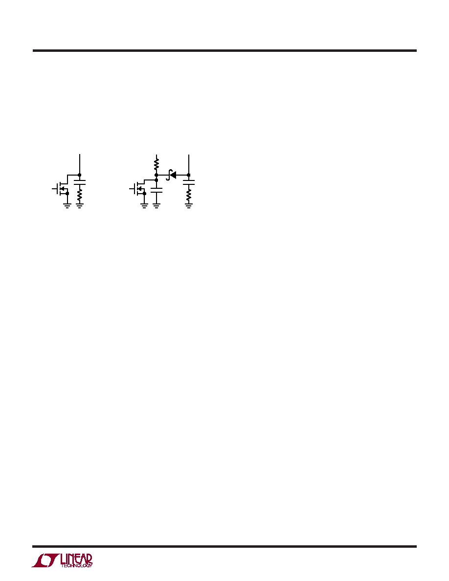
During normal operation the voltage on the ITH/RUN pin
will vary from 1.25V to 2.25V depending on the load
current. Pulling the ITH/RUN pin below 0.8V puts the
LTC1701 into a low quiescent current shutdown mode
(IQ < 1A). This pin can be driven directly from logic as
shown in Figures 3(a).
continuous mode, IGATECHG = f QP, where QP is the gate
charge of the internal MOSFET switch.
3) I2R Losses are predicted from the DC resistances of the
MOSFET and inductor. In continuous mode the average
output current flows through L, but is “chopped” between
the topside internal MOSFET and the Schottky diode. At
low supply voltages where the switch on-resistance is
higher and the switch is on for longer periods due to the
higher duty cycle, the switch losses will dominate. Using
a larger inductance helps minimize these switch losses. At
high supply voltages, these losses are proportional to the
load. I2R losses cause the efficiency to drop at high output
currents.
4) The Schottky diode is a major source of power loss at
high currents and gets worse at low output voltages. The
diode loss is calculated by multiplying the forward voltage
drop times the diode duty cycle multiplied by the load
current.
Other “hidden” losses such as copper trace and internal
battery resistances can account for additional efficiency
degradations in portable systems. It is very important to
include these “system” level losses in the design of a
system. The internal battery and fuse resistance losses
can be minimized by making sure that CIN has adequate
charge storage and very low ESR at the switching fre-
quency. Other losses including Schottky conduction losses
during dead-time and inductor core losses generally ac-
count for less than 2% total additional loss.
THERMAL CONSIDERATIONS
The power handling capability of the device at high ambi-
ent temperatures will be limited by the maximum rated
junction temperature (125
°C). It is important to give
careful consideration to all sources of thermal resistance
from junction to ambient. Additional heat sources mounted
nearby must also be considered.
For surface mount devices, heat sinking is accomplished
by using the heat spreading capabilities of the PC board
and its copper traces. Copper board stiffeners and plated
through-holes can also be used to spread the heat gener-
ated by power devices.
Figure 3. ITH/RUN Pin Interfacing
Efficiency Considerations
The percent efficiency of a switching regulator is equal to
the output power divided by the input power times 100%.
It is often useful to analyze individual losses to determine
what is limiting the efficiency and what change would
produce the most improvement. Percent efficiency can be
expressed as:
%Efficiency = 100% – (L1 + L2 + L3 + ...)
where L1, L2, etc. are the individual losses as a percentage
of input power.
Although all dissipative elements in the circuit produce
losses, 4 main sources usually account for most of the
losses in LTC1701 circuits: 1) LTC1701 VIN current,
2) switching losses, 3) I2R losses, 4) Schottky diode
losses.
1) The VIN current is the DC supply current given in the
electrical characteristics which excludes MOSFET driver
and control currents. VIN current results in a small (< 0.1%)
loss that increases with VIN, even at no load.
2) The switching current is the sum of the internal MOSFET
driver and control currents. The MOSFET driver current
results from switching the gate capacitance of the power
MOSFET. Each time a MOSFET gate is switched from low
to high to low again, a packet of charge dQ moves from VIN
to ground. The resulting dQ/dt is a current out of VIN that
is typically much larger than the control circuit current. In
D1
ITH/RUN
CC
RC
1701 F03
ITH/RUN
CC
RC
C1
R1
(a)
(b)
相关PDF资料 |
PDF描述 |
|---|---|
| LTC1798CS8 | Voltage Reference |
| LTC1798CS8-2.5 | Voltage Reference |
| LTC1864AIS8 | A/D CONVERTER |
| LTC1864CMS8 | A/D CONVERTER |
| LTC1864CS8 | A/D CONVERTER |
相关代理商/技术参数 |
参数描述 |
|---|---|
| LTC1757A-1EMS8 | 功能描述:IC CTRLR RF POWER SINGLE 8MSOP RoHS:否 类别:RF/IF 和 RFID >> RF 电源控制器 IC 系列:- 标准包装:3,000 系列:- RF 型:GSM 频率:450MHz ~ 2GHz 特点:四频带 封装/外壳:8-VFBGA 供应商设备封装:8-MicroSMD(1.51x1.51) 包装:带卷 (TR) 其它名称:LMV243BLX |
| LTC1757A-1EMS8#PBF | 功能描述:IC CTRLR RF POWER SINGLE 8MSOP RoHS:是 类别:RF/IF 和 RFID >> RF 电源控制器 IC 系列:- 标准包装:3,000 系列:- RF 型:GSM 频率:450MHz ~ 2GHz 特点:四频带 封装/外壳:8-VFBGA 供应商设备封装:8-MicroSMD(1.51x1.51) 包装:带卷 (TR) 其它名称:LMV243BLX |
| LTC1757A-1EMS8#TR | 功能描述:IC CTRLR RF POWER SINGLE 8MSOP RoHS:否 类别:RF/IF 和 RFID >> RF 电源控制器 IC 系列:- 标准包装:3,000 系列:- RF 型:GSM 频率:450MHz ~ 2GHz 特点:四频带 封装/外壳:8-VFBGA 供应商设备封装:8-MicroSMD(1.51x1.51) 包装:带卷 (TR) 其它名称:LMV243BLX |
| LTC1757A-1EMS8#TRPBF | 功能描述:IC CTRLR RF POWER SINGLE 8MSOP RoHS:是 类别:RF/IF 和 RFID >> RF 电源控制器 IC 系列:- 标准包装:3,000 系列:- RF 型:GSM 频率:450MHz ~ 2GHz 特点:四频带 封装/外壳:8-VFBGA 供应商设备封装:8-MicroSMD(1.51x1.51) 包装:带卷 (TR) 其它名称:LMV243BLX |
| LTC1757A-2EMS | 功能描述:IC CTRLR RF POWER DUAL 10MSOP RoHS:否 类别:RF/IF 和 RFID >> RF 电源控制器 IC 系列:- 标准包装:3,000 系列:- RF 型:GSM 频率:450MHz ~ 2GHz 特点:四频带 封装/外壳:8-VFBGA 供应商设备封装:8-MicroSMD(1.51x1.51) 包装:带卷 (TR) 其它名称:LMV243BLX |
发布紧急采购,3分钟左右您将得到回复。