- 您现在的位置:买卖IC网 > PDF目录15326 > LTC1772HS6#TRMPBF (Linear Technology)IC REG CTRLR BUCK PWM CM SOT23-6 PDF资料下载
参数资料
| 型号: | LTC1772HS6#TRMPBF |
| 厂商: | Linear Technology |
| 文件页数: | 6/12页 |
| 文件大小: | 0K |
| 描述: | IC REG CTRLR BUCK PWM CM SOT23-6 |
| 标准包装: | 500 |
| PWM 型: | 电流模式 |
| 输出数: | 1 |
| 频率 - 最大: | 650kHz |
| 占空比: | 100% |
| 电源电压: | 2.5 V ~ 9.8 V |
| 降压: | 是 |
| 升压: | 无 |
| 回扫: | 无 |
| 反相: | 无 |
| 倍增器: | 无 |
| 除法器: | 无 |
| Cuk: | 无 |
| 隔离: | 无 |
| 工作温度: | -40°C ~ 140°C |
| 封装/外壳: | SOT-23-6 细型,TSOT-23-6 |
| 包装: | 带卷 (TR) |
�� �
�
�LTC1772�
�OPERATIO�
�(Refer� to� Functional� Diagram)�
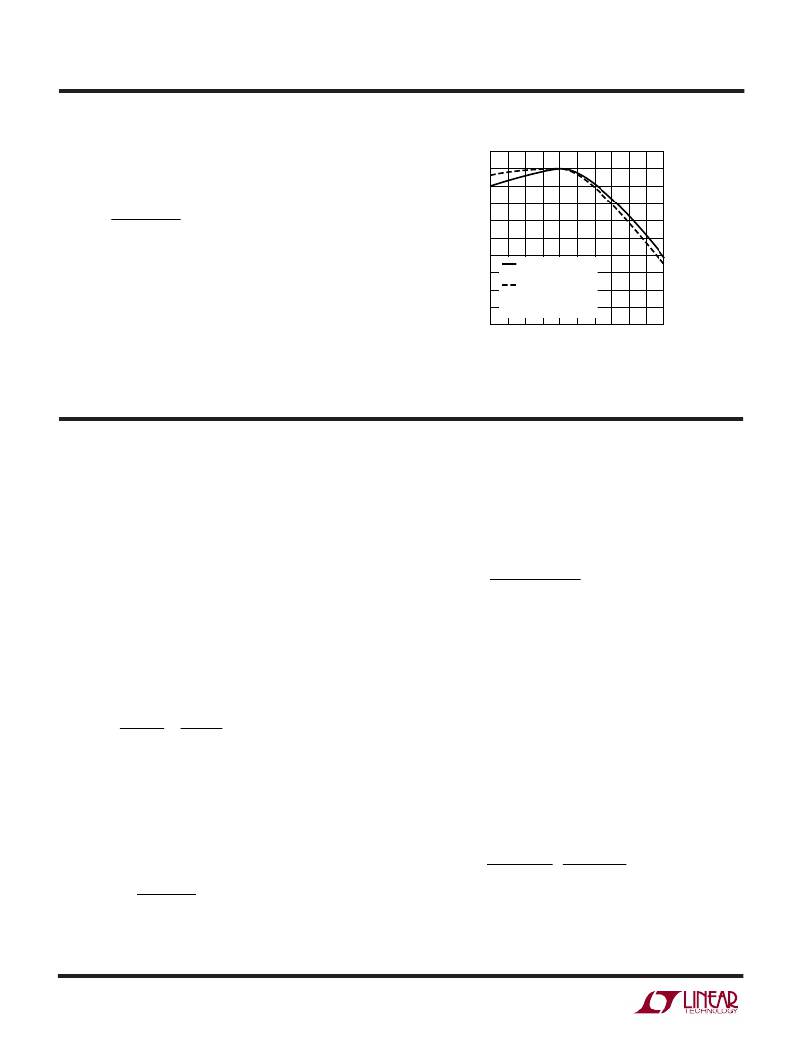
�Slope� Compensation� and� Inductor’s� Peak� Current�
�The� inductor’s� peak� current� is� determined� by:�
�110�
�100�
�90�
�I� PK� =�
�V� ITH� –� 0� .� 7�
�10� (� R� SENSE� )�
�80�
�70�
�60�
�when� the� LTC1772� is� operating� below� 40%� duty� cycle.�
�However,� once� the� duty� cycle� exceeds� 40%,� slope� com-�
�pensation� begins� and� effectively� reduces� the� peak� induc-�
�tor� current.� The� amount� of� reduction� is� given� by� the� curves�
�in� Figure� 2.�
�50�
�40�
�30�
�20�
�10�
�0�
�I� RIPPLE� =� 0.4I� PK�
�AT� 5%� DUTY� CYCLE�
�I� RIPPLE� =� 0.2I� PK�
�AT� 5%� DUTY� CYCLE�
�V� IN� =� 4.2V�
�10� 20� 30� 40� 50� 60� 70� 80� 90� 100�
�DUTY� CYCLE� (%)�
�1772� F02�
�Figure� 2.� Maximum� Output� Current� vs� Duty� Cycle�
�APPLICATIO� N� S� I� N� FOR� M� ATIO� N�
�R� SENSE� =�
�ThebasicLTC1772applicationcircuitisshownin Figure 1.�
�External� component� selection� is� driven� by� the� load� re-�
�quirement� and� begins� with� the� selection� of� L1� and� R� SENSE�
�(=� R1).� Next,� the� power� MOSFET,� M1� and� the� output� diode�
�D1� are� selected� followed� by� C� IN� (=� C1)� and� C� OUT� (=� C2).�
�R� SENSE� Selection� for� Output� Current�
�R� SENSE� is� chosen� based� on� the� required� output� current.�
�With� the� current� comparator� monitoring� the� voltage� devel-�
�oped� across� R� SENSE� ,� the� threshold� of� the� comparator�
�determines� the� inductor’s� peak� current.� The� output� cur-�
�rent� the� LTC1772� can� provide� is� given� by:�
�However,� for� operation� that� is� above� 40%� duty� cycle,� slope�
�compensation� effect� has� to� be� taken� into� consideration� to�
�select� the� appropriate� value� to� provide� the� required� amount�
�of� current.� Using� Figure� 2,� the� value� of� R� SENSE� is:�
�SF�
�(� 10� )(� I� OUT� )(� 100� )�
�Inductor� Value� Calculation�
�The� operating� frequency� and� inductor� selection� are� inter-�
�related� in� that� higher� operating� frequencies� permit� the� use�
�of� a� smaller� inductor� for� the� same� amount� of� inductor�
�?� RIPPLE�
�I� OUT� =�
�0� .� 12�
�R� SENSE�
�I�
�2�
�ripple� current.� However,� this� is� at� the� expense� of� efficiency�
�due� to� an� increase� in� MOSFET� gate� charge� losses.�
�The� inductance� value� also� has� a� direct� effect� on� ripple�
�R� SENSE� =�
�for� Duty� Cycle� <� 40%�
�V� IN� ?� V� OUT� ?� V� OUT� +� V� D� ?�
�?� V� IN� D� ?�
�I� RIPPLE� =� ?� ?�
�where I� RIPPLE� is the inductor peak-to-peak ripple current�
�(see� Inductor� Value� Calculation� section).�
�A� reasonable� starting� point� for� setting� ripple� current� is�
�I� RIPPLE� =� (0.4)(I� OUT� ).� Rearranging� the� above� equation,� it�
�becomes:�
�1�
�(� 10� )(� I� OUT� )�
�current.� The� ripple� current,� I� RIPPLE� ,� decreases� with� higher�
�inductance� or� frequency� and� increases� with� higher� V� IN� or�
�V� OUT� .� The� inductor’s� peak-to-peak� ripple� current� is� given�
�by:�
�f� (� L� )� +� V�
�1772fb�
�6�
�相关PDF资料 |
PDF描述 |
|---|---|
| GSM10DTMN-S273 | CONN EDGECARD 20POS R/A .156 SLD |
| IMC1210BN390J | INDUCTOR WW 39UH 5% 1210 |
| LTC1771EMS8 | IC REG CTRLR BUCK PWM CM 8-MSOP |
| GMM10DTMN-S273 | CONN EDGECARD 20POS R/A .156 SLD |
| VI-JWT-EY-F4 | CONVERTER MOD DC/DC 6.5V 50W |
相关代理商/技术参数 |
参数描述 |
|---|---|
| LTC1772IS6 | 制造商:Linear Technology 功能描述:DC DC Cntrlr Single-OUT Step Down 2.5V to 9.8V Input 6-Pin TSOT-23 |
| LTC1772IS6#PBF | 制造商:Linear Technology 功能描述:DC DC Cntrlr Single-OUT Step Down 2.5V to 9.8V Input 6-Pin TSOT-23 |
| LTC1772IS6#TR | 功能描述:IC REG CTRLR BUCK PWM CM SOT23-6 RoHS:否 类别:集成电路 (IC) >> PMIC - 稳压器 - DC DC 切换控制器 系列:- 标准包装:2,500 系列:- PWM 型:电流模式 输出数:1 频率 - 最大:500kHz 占空比:96% 电源电压:4 V ~ 36 V 降压:无 升压:是 回扫:无 反相:无 倍增器:无 除法器:无 Cuk:无 隔离:无 工作温度:-40°C ~ 125°C 封装/外壳:24-WQFN 裸露焊盘 包装:带卷 (TR) |
| LTC1772IS6#TRM | 功能描述:IC REG CTRLR BUCK PWM CM SOT23-6 RoHS:否 类别:集成电路 (IC) >> PMIC - 稳压器 - DC DC 切换控制器 系列:- 标准包装:2,500 系列:- PWM 型:电流模式 输出数:1 频率 - 最大:500kHz 占空比:96% 电源电压:4 V ~ 36 V 降压:无 升压:是 回扫:无 反相:无 倍增器:无 除法器:无 Cuk:无 隔离:无 工作温度:-40°C ~ 125°C 封装/外壳:24-WQFN 裸露焊盘 包装:带卷 (TR) |
| LTC1772IS6#TRMPBF | 功能描述:IC REG CTRLR BUCK PWM CM SOT23-6 RoHS:是 类别:集成电路 (IC) >> PMIC - 稳压器 - DC DC 切换控制器 系列:- 标准包装:2,500 系列:- PWM 型:电流模式 输出数:1 频率 - 最大:500kHz 占空比:96% 电源电压:4 V ~ 36 V 降压:无 升压:是 回扫:无 反相:无 倍增器:无 除法器:无 Cuk:无 隔离:无 工作温度:-40°C ~ 125°C 封装/外壳:24-WQFN 裸露焊盘 包装:带卷 (TR) |
发布紧急采购,3分钟左右您将得到回复。