- 您现在的位置:买卖IC网 > PDF目录10788 > LTC1821BCGW#TRPBF (Linear Technology)IC D/A CONV 16BIT PRECISE 36SSOP PDF资料下载
参数资料
| 型号: | LTC1821BCGW#TRPBF |
| 厂商: | Linear Technology |
| 文件页数: | 4/16页 |
| 文件大小: | 0K |
| 描述: | IC D/A CONV 16BIT PRECISE 36SSOP |
| 产品培训模块: | LTC275x 18-Bit DAC |
| 标准包装: | 1,000 |
| 设置时间: | 2µs |
| 位数: | 16 |
| 数据接口: | 并联 |
| 转换器数目: | 1 |
| 电压电源: | 单电源 |
| 工作温度: | 0°C ~ 70°C |
| 安装类型: | 表面贴装 |
| 封装/外壳: | 36-BSOP(0.295",7.50mm 宽) |
| 供应商设备封装: | 36-SSOP |
| 包装: | 带卷 (TR) |
| 输出数目和类型: | 1 电压,单极;1 电压,双极 |
| 采样率(每秒): | * |
12
LTC1821
Precision Voltage Reference Considerations
Because of the extremely high accuracy of the 16-bit
LTC1821, careful thought should be given to the selection
of a precision voltage reference. As shown in the section
describing the basic operation of the LTC1821, the output
voltage of the DAC circuit is directly affected by the voltage
reference; thus, any voltage reference error will appear as
a DAC output voltage error.
There are three primary error sources to consider when
selecting a precision voltage reference for 16-bit applica-
tions: output voltage initial tolerance, output voltage tem-
perature coefficient (TC), and output voltage noise.
Initial reference output voltage tolerance, if uncorrected,
generates a full-scale error term. Choosing a reference
with low output voltage initial tolerance, like the LT1236
(
±0.05%), minimizes the gain error due to the reference;
however, a calibration sequence that corrects for system
zero- and full-scale error is always recommended.
A reference’s output voltage temperature coefficient af-
fects not only the full-scale error, but can also affect the
circuit’s INL and DNL performance. If a reference is
chosen with a loose output voltage temperature coeffi-
cient, then the DAC output voltage along its transfer
characteristic will be very dependent on ambient condi-
tions. Minimizing the error due to reference temperature
coefficient can be achieved by choosing a precision refer-
ence with a low output voltage temperature coefficient
and/or tightly controlling the ambient temperature of the
circuit to minimize temperature gradients.
As precision DAC applications move to 16-bit and higher
performance, reference output voltage noise may contrib-
ute a dominant share of the system’s noise floor. This in
turn can degrade system dynamic range and signal-to-
noise ratio. Care should be exercised in selecting a voltage
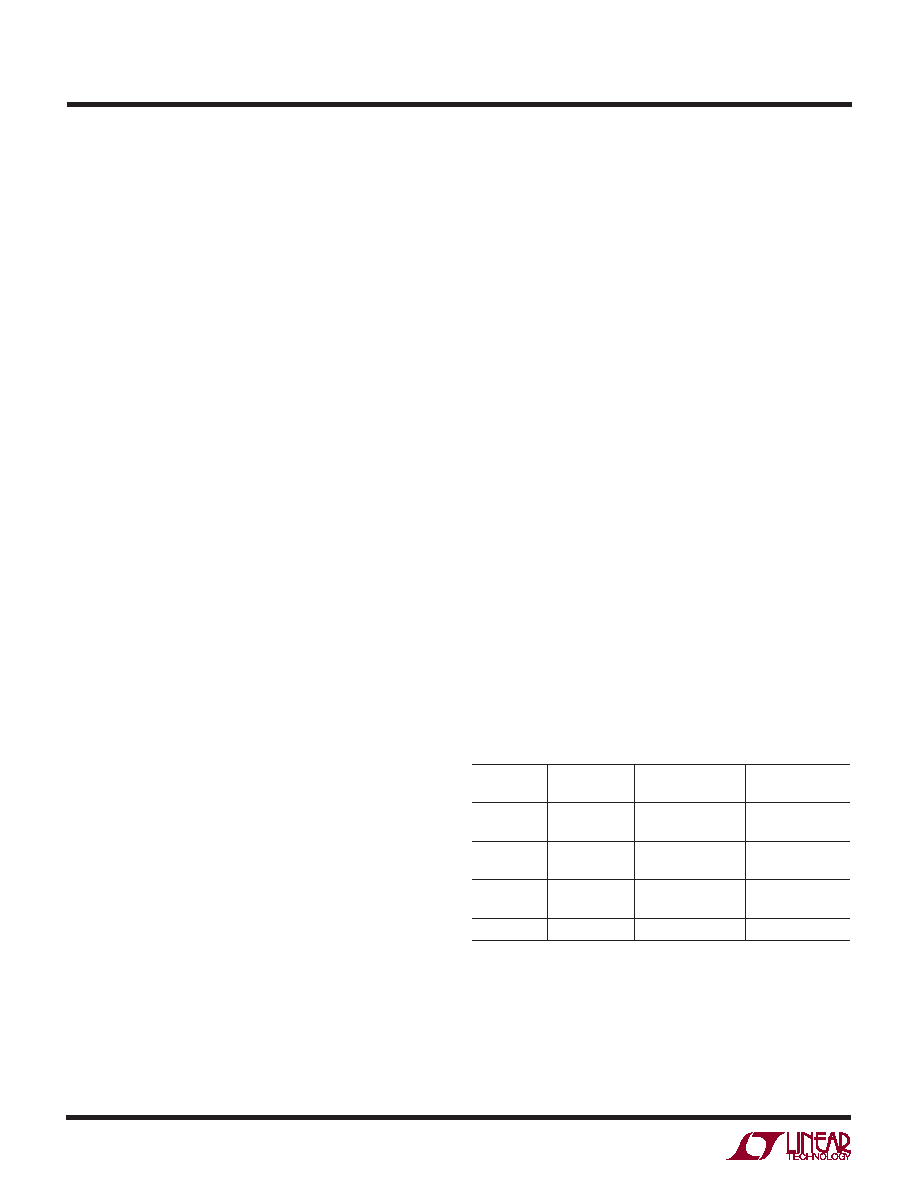
Table 2. Partial List of LTC Precision References Recommended
for Use with the LTC1821, with Relevant Specifications
INITIAL
TEMPERATURE
0.1Hz to 10Hz
REFERENCE
TOLERANCE
DRIFT
NOISE
LT1019A-5,
±0.05%
5ppm/
°C12VP-P
LT1019A-10
LT1236A-5,
±0.05%
5ppm/
°C3VP-P
LT1236A-10
LT1460A-5,
±0.075%
10ppm/
°C20VP-P
LT1460A-10
LT1790A-2.5
±0.05%
10ppm/
°C12VP-P
APPLICATIONS INFORMATION
WU
U
reference with as low an output noise voltage as practical
for the system resolution desired. Precision voltage refer-
ences, like the LT1236, produce low output noise in the
0.1Hz to 10Hz region, well below the 16-bit LSB level in 5V
or 10V full-scale systems. However, as the circuit band-
widths increase, filtering the output of the reference may
be required to minimize output noise.
Grounding
As with any high resolution converter, clean grounding is
important. A low impedance analog ground plane and star
grounding should be used. AGNDF and AGNDS must be
tied to the star ground with as low a resistance as possible.
When it is not possible to locate star ground close to
AGNDF and AGNDS, separate traces should be used to
route these pins to the star ground. This minimizes the
voltage drop from these pins to ground due to the code
dependent current flowing into the ground plane. If the
resistance of these separate circuit board traces exceeds
1
, the circuit of Figure 3 eliminates this code dependent
voltage drop error for high resistance traces.
To calculate PC track resistance in squares, divide the
length of the PC track by the width and multiply this result
by the sheet resistance of copper foil. For 1 oz copper
(
≈1.4 mils thick), the sheet resistance is 0.045 per
square.
相关PDF资料 |
PDF描述 |
|---|---|
| FGN.1M.308.XLCT | CONN PLUG 8POS STRGHT PIN CRIMP |
| LTC1821BIGW#TRPBF | IC D/A CONV 16BIT PRECISE 36SSOP |
| VI-24H-CU-F1 | CONVERTER MOD DC/DC 52V 200W |
| LTC1821AIGW#TRPBF | IC D/A CONV 16BIT PRECISE 36SSOP |
| LTC1458LCSW#TRPBF | IC D/A CONV 12BIT R-R QUAD28SOIC |
相关代理商/技术参数 |
参数描述 |
|---|---|
| LTC1821BIGW | 功能描述:IC D/A CONV 16BIT PRECISE 36SSOP RoHS:否 类别:集成电路 (IC) >> 数据采集 - 数模转换器 系列:- 产品培训模块:Lead (SnPb) Finish for COTS Obsolescence Mitigation Program 标准包装:1,000 系列:- 设置时间:1µs 位数:8 数据接口:串行 转换器数目:8 电压电源:双 ± 功率耗散(最大):941mW 工作温度:0°C ~ 70°C 安装类型:表面贴装 封装/外壳:24-SOIC(0.295",7.50mm 宽) 供应商设备封装:24-SOIC W 包装:带卷 (TR) 输出数目和类型:8 电压,单极 采样率(每秒):* |
| LTC1821BIGW#PBF | 功能描述:IC D/A CONV 16BIT PRECISE 36SSOP RoHS:是 类别:集成电路 (IC) >> 数据采集 - 数模转换器 系列:- 标准包装:2,400 系列:- 设置时间:- 位数:18 数据接口:串行 转换器数目:3 电压电源:模拟和数字 功率耗散(最大):- 工作温度:-40°C ~ 85°C 安装类型:表面贴装 封装/外壳:36-TFBGA 供应商设备封装:36-TFBGA 包装:带卷 (TR) 输出数目和类型:* 采样率(每秒):* |
| LTC1821BIGW#TR | 功能描述:IC D/A CONV 16BIT PRECISE 36SSOP RoHS:否 类别:集成电路 (IC) >> 数据采集 - 数模转换器 系列:- 产品培训模块:Lead (SnPb) Finish for COTS Obsolescence Mitigation Program 标准包装:1,000 系列:- 设置时间:1µs 位数:8 数据接口:串行 转换器数目:8 电压电源:双 ± 功率耗散(最大):941mW 工作温度:0°C ~ 70°C 安装类型:表面贴装 封装/外壳:24-SOIC(0.295",7.50mm 宽) 供应商设备封装:24-SOIC W 包装:带卷 (TR) 输出数目和类型:8 电压,单极 采样率(每秒):* |
| LTC1821BIGW#TRPBF | 功能描述:IC D/A CONV 16BIT PRECISE 36SSOP RoHS:是 类别:集成电路 (IC) >> 数据采集 - 数模转换器 系列:- 标准包装:2,400 系列:- 设置时间:- 位数:18 数据接口:串行 转换器数目:3 电压电源:模拟和数字 功率耗散(最大):- 工作温度:-40°C ~ 85°C 安装类型:表面贴装 封装/外壳:36-TFBGA 供应商设备封装:36-TFBGA 包装:带卷 (TR) 输出数目和类型:* 采样率(每秒):* |
| LTC1840CGN | 功能描述:IC DUAL FAN CONTROLLER 16-SSOP RoHS:否 类别:集成电路 (IC) >> PMIC - 电机和风扇控制器,驱动器 系列:- 产品变化通告:ATA683(3,4)PLQW Obsolescence 09/Aug/2012 标准包装:1 系列:- 应用:DC 电机控制器,无刷(BLDC),3 相 评估套件:可供 输出数:1 电流 - 输出:100mA 电压 - 负载:5.25 V ~ 20 V 电源电压:5.25 V ~ 20 V 工作温度:-40°C ~ 150°C 安装类型:表面贴装 封装/外壳:48-VFQFN 裸露焊盘 供应商设备封装:48-VQFN(7x7) 包装:剪切带 (CT) 其它名称:ATA6833-PLQWCT |
发布紧急采购,3分钟左右您将得到回复。