- 您现在的位置:买卖IC网 > PDF目录10796 > LTC1842CS8#PBF (Linear Technology)IC COMP ULTLOPWR W/REF DUAL8SOIC PDF资料下载
参数资料
| 型号: | LTC1842CS8#PBF |
| 厂商: | Linear Technology |
| 文件页数: | 10/12页 |
| 文件大小: | 0K |
| 描述: | IC COMP ULTLOPWR W/REF DUAL8SOIC |
| 标准包装: | 100 |
| 类型: | 带电压基准 |
| 元件数: | 2 |
| 输出类型: | 开路漏极 |
| 电压 - 电源,单路/双路(±): | 2.5 V ~ 11 V,±1.25 V ~ 5.5 V |
| 电压 - 输入偏移(最小值): | 10mV @ 5V |
| 电流 - 静态(最大值): | 5.7µA |
| CMRR, PSRR(标准): | 80dB CMRR,80dB PSRR |
| 传输延迟(最大): | 12µs |
| 磁滞: | 50mV |
| 工作温度: | 0°C ~ 70°C |
| 封装/外壳: | 8-SOIC(0.154",3.90mm 宽) |
| 安装类型: | 表面贴装 |
| 包装: | 管件 |
| 产品目录页面: | 1324 (CN2011-ZH PDF) |
7
LTC1841/LTC1842/LTC1843
APPLICATIONS INFORMATION
WU
U
The LTC1841/LTC1842/LTC1843 are dual micropower
comparators with a built-in 1.182V reference (LTC1842/
LTC1843). Features include programmable hysteresis,
wide supply voltage range (2V to 11V) and the ability for
the reference to drive up to a 0.01
F capacitor without
oscillation. The comparators’ open-drain outputs can typi-
cally sink greater than 20mA and the supply current
glitches that normally occur when switching logic states
have been eliminated.
Power Supplies
The comparators operate from a single 2V to 11V (2.5V to
11V for LTC1842/LTC1843) or dual
±1V to ±5.5V supply
(
±1.25V to ±5.5V for LTC1842/LTC1843). If the reference
output is required to source more than 1mA or the supply
source impedance is high, V + should be bypassed with a
0.1
F capacitor.
Comparator Inputs
The comparators’ input can swing from the negative
supply V – to within 1.3V (max) of the positive supply V +.
The input can be forced 300mV below V – or above V +
without damage and the typical input leakage current is
only
±10pA.
Comparator Outputs
Each comparator output is an open-drain pull-down to V–
typically capable of sinking greater than 20mA. The low
output leakage current while in three-state mode allows a
high value pull-up resistor to be used. The open-drain
outputs can be wire OR-ed or used in level shifting
applications.
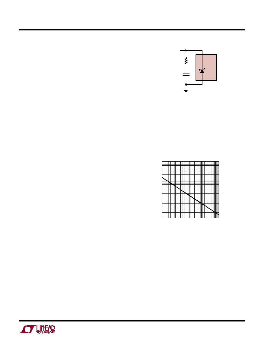
Voltage Reference
The internal bandgap reference has an output voltage of
1.182V referenced to V –. The reference accuracy is 1.5%
from – 40
°C to 85°C. It can typically source greater than
1mA and sink up to 10
A with a 5V supply. The reference
can drive a bypass capacitor of up to 0.01
F without
oscillation. By inserting a series resistor, capacitance
values up to 100
F can be used (Figure 1).
Figure 1. Damping the Reference Output
Figure 3 shows the bypassed reference output with a
square wave applied to the V + pin. Resistors R2 and R3 set
a 10mV hysteresis voltage band while R1 damps the
reference response. Note that the comparator output
doesn’t trip.
CAPACITOR VALUE (
F)
0.001
0.1
RESISTOR
VALUE
(k
)
10
0.01
0.1
10
1
1841/43 F02
1
100
Figure 2. Damping Resistance vs Bypass Capacitor Value
LTC1843
V –
REF
R1
C1
REFERENCE
OUTPUT
1841/43 F01
Figure 2 shows the resistor value required for different
capacitor values to achieve critical damping. Bypassing
the reference can help prevent false tripping of the com-
parators by preventing glitches on V + or reference load
transients from disturbing the reference output voltage.
相关PDF资料 |
PDF描述 |
|---|---|
| ADM233LANZ | IC TX/RX DUAL RS-232 5VLP 20DIP |
| AD7545KN | IC DAC 12BIT W/BUFF MULT 20-DIP |
| LTC1440CN8#PBF | IC COMP W/REF LP SINGLE 8-DIP |
| LTC491CS#PBF | IC TXRX RS485 LOW POWER 14-SOIC |
| AD7545ALN | IC DAC 12BIT W/BUFF MULT 20-DIP |
相关代理商/技术参数 |
参数描述 |
|---|---|
| LTC1842IS8 | 功能描述:IC COMP ULTLOPWR W/REF DUAL8SOIC RoHS:否 类别:集成电路 (IC) >> 线性 - 比较器 系列:- 标准包装:25 系列:- 类型:带电压基准 元件数:4 输出类型:CMOS,开路漏极,TTL 电压 - 电源,单路/双路(±):2 V ~ 11 V,±1 V ~ 5.5 V 电压 - 输入偏移(最小值):10mV @ 5V 电流 - 输入偏压(最小值):- 电流 - 输出(标准):0.015mA @ 5V 电流 - 静态(最大值):8.5µA CMRR, PSRR(标准):80dB CMRR,80dB PSRR 传输延迟(最大):12µs 磁滞:50mV 工作温度:0°C ~ 70°C 封装/外壳:16-DIP(0.300",7.62mm) 安装类型:通孔 包装:管件 |
| LTC1842IS8#PBF | 功能描述:IC COMP ULTLOPWR W/REF DL 8SOIC RoHS:是 类别:集成电路 (IC) >> 线性 - 比较器 系列:- 标准包装:25 系列:- 类型:带电压基准 元件数:4 输出类型:CMOS,开路漏极,TTL 电压 - 电源,单路/双路(±):2 V ~ 11 V,±1 V ~ 5.5 V 电压 - 输入偏移(最小值):10mV @ 5V 电流 - 输入偏压(最小值):- 电流 - 输出(标准):0.015mA @ 5V 电流 - 静态(最大值):8.5µA CMRR, PSRR(标准):80dB CMRR,80dB PSRR 传输延迟(最大):12µs 磁滞:50mV 工作温度:0°C ~ 70°C 封装/外壳:16-DIP(0.300",7.62mm) 安装类型:通孔 包装:管件 |
| LTC1842IS8#TR | 功能描述:IC COMPARATOR DUAL ULT LP 8SOIC RoHS:否 类别:集成电路 (IC) >> 线性 - 比较器 系列:- 标准包装:25 系列:- 类型:带电压基准 元件数:4 输出类型:CMOS,开路漏极,TTL 电压 - 电源,单路/双路(±):2 V ~ 11 V,±1 V ~ 5.5 V 电压 - 输入偏移(最小值):10mV @ 5V 电流 - 输入偏压(最小值):- 电流 - 输出(标准):0.015mA @ 5V 电流 - 静态(最大值):8.5µA CMRR, PSRR(标准):80dB CMRR,80dB PSRR 传输延迟(最大):12µs 磁滞:50mV 工作温度:0°C ~ 70°C 封装/外壳:16-DIP(0.300",7.62mm) 安装类型:通孔 包装:管件 |
| LTC1842IS8#TRPBF | 功能描述:IC COMP ULTLOPWR W/REF DL 8SOIC RoHS:是 类别:集成电路 (IC) >> 线性 - 比较器 系列:- 标准包装:25 系列:- 类型:带电压基准 元件数:4 输出类型:CMOS,开路漏极,TTL 电压 - 电源,单路/双路(±):2 V ~ 11 V,±1 V ~ 5.5 V 电压 - 输入偏移(最小值):10mV @ 5V 电流 - 输入偏压(最小值):- 电流 - 输出(标准):0.015mA @ 5V 电流 - 静态(最大值):8.5µA CMRR, PSRR(标准):80dB CMRR,80dB PSRR 传输延迟(最大):12µs 磁滞:50mV 工作温度:0°C ~ 70°C 封装/外壳:16-DIP(0.300",7.62mm) 安装类型:通孔 包装:管件 |
| LTC1843CS8 | 功能描述:IC COMP ULTLOPWR W/REF DUAL8SOIC RoHS:否 类别:集成电路 (IC) >> 线性 - 比较器 系列:- 产品培训模块:Lead (SnPb) Finish for COTS Obsolescence Mitigation Program 标准包装:50 系列:- 类型:带电压基准 元件数:4 输出类型:开路漏极 电压 - 电源,单路/双路(±):2.5 V ~ 11 V,±1.25 V ~ 5.5 V 电压 - 输入偏移(最小值):10mV @ 5V 电流 - 输入偏压(最小值):- 电流 - 输出(标准):0.015mA @ 5V 电流 - 静态(最大值):8.5µA CMRR, PSRR(标准):80dB CMRR,80dB PSRR 传输延迟(最大):- 磁滞:- 工作温度:0°C ~ 70°C 封装/外壳:16-SOIC(0.154",3.90mm 宽) 安装类型:表面贴装 包装:管件 产品目录页面:1386 (CN2011-ZH PDF) |
发布紧急采购,3分钟左右您将得到回复。