- 您现在的位置:买卖IC网 > PDF目录10288 > LTC1850CFW#TRPBF (Linear Technology)IC ADC 10BIT 1.25MSPS 48-TSSOP PDF资料下载
参数资料
| 型号: | LTC1850CFW#TRPBF |
| 厂商: | Linear Technology |
| 文件页数: | 7/28页 |
| 文件大小: | 0K |
| 描述: | IC ADC 10BIT 1.25MSPS 48-TSSOP |
| 标准包装: | 1,800 |
| 位数: | 10 |
| 采样率(每秒): | 1.25M |
| 数据接口: | 并联 |
| 转换器数目: | 1 |
| 功率耗散(最大): | 50mW |
| 电压电源: | 单电源 |
| 工作温度: | 0°C ~ 70°C |
| 安装类型: | 表面贴装 |
| 封装/外壳: | 48-TFSOP(0.240",6.10mm 宽) |
| 供应商设备封装: | 48-TSSOP |
| 包装: | 带卷 (TR) |
| 输入数目和类型: | 8 个单端,单极;8 个单端,双极;4 个差分,单极;4 个差分,双极 |
第1页第2页第3页第4页第5页第6页当前第7页第8页第9页第10页第11页第12页第13页第14页第15页第16页第17页第18页第19页第20页第21页第22页第23页第24页第25页第26页第27页第28页
15
LTC1850/LTC1851
18501f
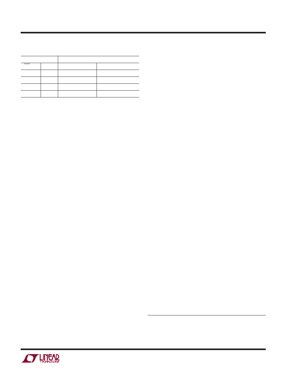
Table 2. Input Span Table
INPUT SPAN
UNI/BIP
PGA
REFCOMP = 4.096V
0
0 – REFCOMP/2
0 – 2.048V
0
1
0 – REFCOMP
0 – 4.096V
10
±REFCOMP/4
±1.024V
11
±REFCOMP/2
±2.048V
It should be noted that the bipolar input span of the
LTC1850/LTC1851 does not allow negative inputs with
respect to ground. The LTC1850/LTC1851 have a unique
differential sample-and-hold circuit that allows rail-to-rail
inputs. The ADC will always convert the difference of the
“+” and “–” inputs independent of the common mode
voltage. The common mode rejection holds up to high
frequencies. The only requirement is that both inputs can
not exceed the VDD power supply voltage or ground. When
a bipolar input span is selected the “+” input can swing
±full scale relative to the “–” input but neither input can
exceed VDD or go below ground.
Integral nonlinearity errors (INL) and differential nonlin-
earity errors (DNL) are independent of the common mode
voltage, however, the bipolar zero error (BZE) will vary.
The change in BZE is typically less than 0.1% of the
common mode voltage.
Some AC applications may have their performance lim-
ited by distortion. The ADC and many other circuits exhibit
higher distortion when signals approach the supply or
ground. THD will degrade as the inputs approach either
power supply rail. Distortion can be reduced by reducing
the signal amplitude and keeping the common mode
voltage at approximately midsupply.
Driving the Analog Inputs
The inputs of the LTC1850/LTC1851 are easy to drive.
Each of the analog inputs can be used as a single-ended
input relative to the input common pin (CH0-COM, CH1-
COM, etc.) or in pairs (CH0 and CH1, CH2 and CH3, CH4
and CH5, CH6 and CH7) for differential inputs. Regardless
of the MUX configuration, the “+” and “–” inputs are
sampled at the same instant. Any unwanted signal that is
common mode to both inputs will be reduced by the
common mode rejection of the sample-and-hold circuit.
The inputs draw only one small current spike while charg-
ing the sample-and-hold capacitors at the end of conver-
sion. During conversion, the analog inputs draw only a
small leakage current. If the source impedance of the
driving circuit is low, then the LTC1850/LTC1851 inputs
can be driven directly. As source impedance increases, so
will acquisition time. For minimum acquisition time with
high source impedance, a buffer amplifier should be used.
The only requirement is that the amplifier driving the
analog input(s) must settle after the small current spike
before the next conversion starts (settling time must be
150ns for full throughput rate).
Choosing an Input Amplifier
Choosing an input amplifier is easy if a few requirements
are taken into consideration. First, to limit the magnitude
of the voltage spike seen by the amplifier from charging
the sampling capacitor, choose an amplifier that has a low
output impedance (<100
) at the closed-loop bandwidth
frequency. For example, if an amplifier is used in a gain of
+1 and has a unity-gain bandwidth of 50MHz, then the
output impedance at 50MHz should be less than 100
.
The second requirement is that the closed-loop bandwidth
must be greater than 20MHz to ensure adequate small-
signal settling for full throughput rate. The following list is
a summary of the op amps that are suitable for driving the
LTC1850/LTC1851, more detailed information is available
in the Linear Technology Databooks, the LinearView
TM
CD-ROM and on our web site at www.linear-tech.com.
LT
1360: 50MHz Voltage Feedback Amplifier.
±2.5V to
±15V supplies. 5mA supply current. Low distortion.
LT1363: 70MHz Voltage Feedback Amplifier.
±2.5V to
±15V supplies. 7.5mA supply current. Low distortion.
LT1364/LT1365: Dual and Quad 70MHz Voltage Feedback
Amplifiers.
±2.5V to ±15V supplies. 7.5mA supply current
per amplifier. Low distortion.
APPLICATIO S I FOR ATIO
WU
UU
LinearView is a trademark of Linear Technology Corporation.
相关PDF资料 |
PDF描述 |
|---|---|
| VE-20K-MX-S | CONVERTER MOD DC/DC 40V 75W |
| VE-B64-IX-B1 | CONVERTER MOD DC/DC 48V 75W |
| VE-B6X-MW-S | CONVERTER MOD DC/DC 5.2V 100W |
| R3FZ | CONN PLUG AUDIO 3POS R/A FEMALE |
| VE-B6W-MW-S | CONVERTER MOD DC/DC 5.5V 100W |
相关代理商/技术参数 |
参数描述 |
|---|---|
| LTC1850IFW | 功能描述:IC ADC 10BIT 1.25MSPS 48-TSSOP RoHS:否 类别:集成电路 (IC) >> 数据采集 - 模数转换器 系列:- 标准包装:1,000 系列:- 位数:16 采样率(每秒):45k 数据接口:串行 转换器数目:2 功率耗散(最大):315mW 电压电源:模拟和数字 工作温度:0°C ~ 70°C 安装类型:表面贴装 封装/外壳:28-SOIC(0.295",7.50mm 宽) 供应商设备封装:28-SOIC W 包装:带卷 (TR) 输入数目和类型:2 个单端,单极 |
| LTC1850IFW#PBF | 功能描述:IC ADC 10BIT 1.25MSPS 48-TSSOP RoHS:是 类别:集成电路 (IC) >> 数据采集 - 模数转换器 系列:- 标准包装:1,000 系列:- 位数:16 采样率(每秒):45k 数据接口:串行 转换器数目:2 功率耗散(最大):315mW 电压电源:模拟和数字 工作温度:0°C ~ 70°C 安装类型:表面贴装 封装/外壳:28-SOIC(0.295",7.50mm 宽) 供应商设备封装:28-SOIC W 包装:带卷 (TR) 输入数目和类型:2 个单端,单极 |
| LTC1850IFW#TR | 功能描述:IC ADC 10BIT 1.25MSPS 48-TSSOP RoHS:否 类别:集成电路 (IC) >> 数据采集 - 模数转换器 系列:- 标准包装:1,000 系列:- 位数:16 采样率(每秒):45k 数据接口:串行 转换器数目:2 功率耗散(最大):315mW 电压电源:模拟和数字 工作温度:0°C ~ 70°C 安装类型:表面贴装 封装/外壳:28-SOIC(0.295",7.50mm 宽) 供应商设备封装:28-SOIC W 包装:带卷 (TR) 输入数目和类型:2 个单端,单极 |
| LTC1850IFW#TRPBF | 功能描述:IC ADC 10BIT 1.25MSPS 48-TSSOP RoHS:是 类别:集成电路 (IC) >> 数据采集 - 模数转换器 系列:- 标准包装:1,000 系列:- 位数:16 采样率(每秒):45k 数据接口:串行 转换器数目:2 功率耗散(最大):315mW 电压电源:模拟和数字 工作温度:0°C ~ 70°C 安装类型:表面贴装 封装/外壳:28-SOIC(0.295",7.50mm 宽) 供应商设备封装:28-SOIC W 包装:带卷 (TR) 输入数目和类型:2 个单端,单极 |
| LTC1851CFW | 功能描述:IC ADC 12BIT 1.25MSPS 48-TSSOP RoHS:否 类别:集成电路 (IC) >> 数据采集 - 模数转换器 系列:- 标准包装:1,000 系列:- 位数:12 采样率(每秒):300k 数据接口:并联 转换器数目:1 功率耗散(最大):75mW 电压电源:单电源 工作温度:0°C ~ 70°C 安装类型:表面贴装 封装/外壳:24-SOIC(0.295",7.50mm 宽) 供应商设备封装:24-SOIC 包装:带卷 (TR) 输入数目和类型:1 个单端,单极;1 个单端,双极 |
发布紧急采购,3分钟左右您将得到回复。