- 您现在的位置:买卖IC网 > PDF目录10293 > LTC1852CFW#PBF (Linear Technology)IC ADC 8CH 10BIT 400KSPS 48TSSOP PDF资料下载
参数资料
| 型号: | LTC1852CFW#PBF |
| 厂商: | Linear Technology |
| 文件页数: | 11/24页 |
| 文件大小: | 0K |
| 描述: | IC ADC 8CH 10BIT 400KSPS 48TSSOP |
| 标准包装: | 39 |
| 位数: | 10 |
| 采样率(每秒): | 400k |
| 数据接口: | 并联 |
| 转换器数目: | 1 |
| 功率耗散(最大): | 15mW |
| 电压电源: | 单电源 |
| 工作温度: | 0°C ~ 70°C |
| 安装类型: | 表面贴装 |
| 封装/外壳: | 48-TFSOP(0.240",6.10mm 宽) |
| 供应商设备封装: | 48-TSSOP |
| 包装: | 管件 |
| 输入数目和类型: | 8 个单端,单极;8 个单端,双极;4 个差分,单极;4 个差分,双极 |
LTC1852/LTC1853
19
18523fa
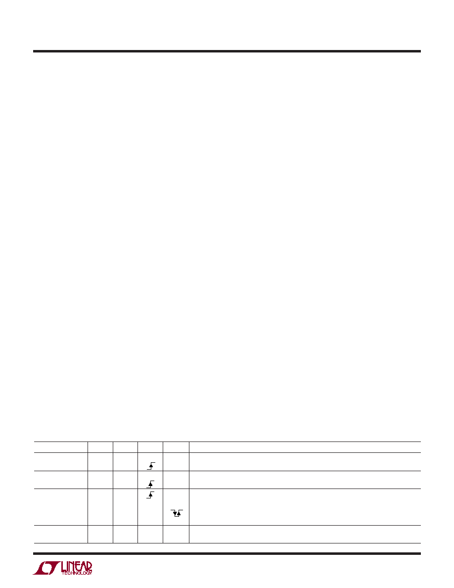
Table 5
OPERATION MODE
M1
M0
WR
RD
COMMENTS
Direct Address
0
OE
Address and Conguration are Driven from External Pins
Address and Conguration are Latched on Rising Edge of WR or Falling Edge of CONVST
Scan
0
1
0
OE
Address is Provided by Internal Scan Counter, Conguration is Driven from External Pins
Conguraton is Latched on Rising Edge of WR or Falling Edge of CONVST
Program
1
0
1
Write Sequencer Location, WR Low Enables Inputs, Rising Edge of WR Latches Data and
Advances to Next Location
Readback
1
0
1
Read Sequencer Location, Falling Edge of RD Enables Output, Rising Edge of RD
Advances to Next Location
Sequence Run
1
X
OE
Run Programmed Sequence, Falling Edge of CONVST Starts Conversion and Advances to
Next Location
The sequencer is accessed by taking the M1 mode pin
high. With M1 high, the sequencer memory is accessed
by taking the M0 mode pin low. This will cause BUSY to
go low, disabling conversions during the programming
and readback of the sequencer. The sequencer is reset
to location 0000 whenever M1 or M0 changes state. One
of these signals should be cycled prior to any read or
write operation to guarantee that the sequencer will be
programmed or read starting at location 0000.
The sequencer is programmed sequentially starting from
location 0000. RD and WR should be held high, the ap-
propriate signals applied to the DIFF pin, the A2 to A0 MUX
address pins, the UNI/BIP pin and the PGA pin and WR
taken low to write to the memory. WR going high will latch
the data into memory and advance the pointer to the next
sequencer location. Up to 16 locations can be programmed
and the last location written before M0 is taken back high
will be the last location in the sequence. After 16 writes,
the pointer is reset to location 0000 and any subsequent
writes will erase all of the previous contents and start a
new sequence.
The sequencer memory can be read by holding WR high
and strobing RD. Taking RD low accesses the sequencer
memory and enables the data output pins. The sequencer
should be reset to location 0000 before beginning a read
operation (by applying a positive pulse to MO). The seven
output bits will be available on the DIFFOUT/S6, A2OUT/S5,
A1OUT/S4, A0OUT/S3, D11/S2, D10/S1 and D9/S0 pins
(LTC1853) or DIFFOUT/S6,A2OUT/S5,A1OUT/S4,A0OUT/S3,
D9/S2, D8/S1 and D7/S0 pins (LTC1852). The D8 to D0
(LTC1853) or D6 to D0 (LTC1852) data output pins will
remain high impedance during readback. RD going high
will return the data output pins to a high impedance state
and advance the pointer to the next location. A logic 1
on the D9/S0 (D7/S0) pin indicates the last location in
the current sequence but all 16 locations can be read by
continuing to clock RD. After 16 reads, the pointer is reset
to location 0000. When all programming and/or reading
of the sequencer memory is complete, M0 is taken high.
BUSYwillcomebackhighenablingCONVSTandindicating
that the part is ready to start a conversion.
Sequence Run Mode
Once the sequencer is programmed, M0 is taken high.
BUSY will also come back high enabling CONVST and
the next falling CONVST will begin a conversion using the
MUX address and input conguration stored in location
0000 of the sequencer memory. After each conversion,
the sequencer pointer is advanced by one and the MUX
address ( the actual channel or channels being converted,
not the sequencer pointer) for the present conversion
is available on the address output pins along with the
conversion result. When the sequencer nishes convert-
ing the last programmed location, the sequencer pointer
will return to location 0000 for the next conversion. The
sequencer will also reset to location 0000 anytime the M1
or M0 pin changes state.
The contents of the sequencer memory will be retained
as long as power is contiuously applied to the part. This
allows the user to switch from Sequence Run mode to
either Direct Address or Scan Mode and back without
losing the programmed sequence. The part can also be
disabled using CS or shutdown in Nap or Sleep mode
without losing the programmed sequence. Table 5 outlines
the operational modes of the LTC1852/LTC1853. Figures 11
and 12 show the timing diagrams for writing to, reading
from and running a sequence.
APPLICATIONS INFORMATION
相关PDF资料 |
PDF描述 |
|---|---|
| VI-B6L-IW-B1 | CONVERTER MOD DC/DC 28V 100W |
| VI-B6K-IX-B1 | CONVERTER MOD DC/DC 40V 75W |
| MS3102R36-3P | CONN RCPT 6POS BOX MNT W/PINS |
| MS27467T25B24B | CONN HSG PLUG 24POS STRGHT SCKT |
| MS27467E25B24SLC | CONN HSG PLUG 24POS STRGHT SCKT |
相关代理商/技术参数 |
参数描述 |
|---|---|
| LTC1852IFW | 功能描述:IC A/D CONV 8CH 10BIT 48-TSSOP RoHS:否 类别:集成电路 (IC) >> 数据采集 - 模数转换器 系列:- 标准包装:1,000 系列:- 位数:16 采样率(每秒):45k 数据接口:串行 转换器数目:2 功率耗散(最大):315mW 电压电源:模拟和数字 工作温度:0°C ~ 70°C 安装类型:表面贴装 封装/外壳:28-SOIC(0.295",7.50mm 宽) 供应商设备封装:28-SOIC W 包装:带卷 (TR) 输入数目和类型:2 个单端,单极 |
| LTC1852IFW#PBF | 功能描述:IC A/D CONV 8CH 10BIT 48-TSSOP RoHS:是 类别:集成电路 (IC) >> 数据采集 - 模数转换器 系列:- 标准包装:1,000 系列:- 位数:16 采样率(每秒):45k 数据接口:串行 转换器数目:2 功率耗散(最大):315mW 电压电源:模拟和数字 工作温度:0°C ~ 70°C 安装类型:表面贴装 封装/外壳:28-SOIC(0.295",7.50mm 宽) 供应商设备封装:28-SOIC W 包装:带卷 (TR) 输入数目和类型:2 个单端,单极 |
| LTC1852IFW#TR | 功能描述:IC A/D CONV 8CH 10BIT 48-TSSOP RoHS:否 类别:集成电路 (IC) >> 数据采集 - 模数转换器 系列:- 标准包装:1,000 系列:- 位数:16 采样率(每秒):45k 数据接口:串行 转换器数目:2 功率耗散(最大):315mW 电压电源:模拟和数字 工作温度:0°C ~ 70°C 安装类型:表面贴装 封装/外壳:28-SOIC(0.295",7.50mm 宽) 供应商设备封装:28-SOIC W 包装:带卷 (TR) 输入数目和类型:2 个单端,单极 |
| LTC1852IFW#TRPBF | 功能描述:IC A/D CONV 8CH 10BIT 48-TSSOP RoHS:是 类别:集成电路 (IC) >> 数据采集 - 模数转换器 系列:- 标准包装:1,000 系列:- 位数:16 采样率(每秒):45k 数据接口:串行 转换器数目:2 功率耗散(最大):315mW 电压电源:模拟和数字 工作温度:0°C ~ 70°C 安装类型:表面贴装 封装/外壳:28-SOIC(0.295",7.50mm 宽) 供应商设备封装:28-SOIC W 包装:带卷 (TR) 输入数目和类型:2 个单端,单极 |
| LTC1853CFW | 功能描述:IC A/D CONV 8CH 12BIT 48-TSSOP RoHS:否 类别:集成电路 (IC) >> 数据采集 - 模数转换器 系列:- 标准包装:1,000 系列:- 位数:16 采样率(每秒):45k 数据接口:串行 转换器数目:2 功率耗散(最大):315mW 电压电源:模拟和数字 工作温度:0°C ~ 70°C 安装类型:表面贴装 封装/外壳:28-SOIC(0.295",7.50mm 宽) 供应商设备封装:28-SOIC W 包装:带卷 (TR) 输入数目和类型:2 个单端,单极 |
发布紧急采购,3分钟左右您将得到回复。