- 您现在的位置:买卖IC网 > PDF目录10292 > LTC1852CFW#TR (Linear Technology)IC A/D CONV 8CH 10BIT 48-TSSOP PDF资料下载
参数资料
| 型号: | LTC1852CFW#TR |
| 厂商: | Linear Technology |
| 文件页数: | 10/24页 |
| 文件大小: | 0K |
| 描述: | IC A/D CONV 8CH 10BIT 48-TSSOP |
| 标准包装: | 1,800 |
| 位数: | 10 |
| 采样率(每秒): | 400k |
| 数据接口: | 并联 |
| 转换器数目: | 1 |
| 功率耗散(最大): | 15mW |
| 电压电源: | 单电源 |
| 工作温度: | 0°C ~ 70°C |
| 安装类型: | 表面贴装 |
| 封装/外壳: | 48-TFSOP(0.240",6.10mm 宽) |
| 供应商设备封装: | 48-TSSOP |
| 包装: | 带卷 (TR) |
| 输入数目和类型: | 8 个单端,单极;8 个单端,双极;4 个差分,单极;4 个差分,双极 |
| 其它名称: | LTC1852CFWTR |
LTC1852/LTC1853
18
18523fa
appear on the data outputs; BUSY goes high releasing the
processor, and the processor takes RD ( = CONVST) back
high and reads the new conversion data.
In ROM mode, the processor takes RD ( = CONVST) low,
starting a conversion and reading the previous conversion
result. After the conversion is complete, the processor can
read the new result and initiate another conversion.
MODES OF OPERATION
Direct Address Mode
The simplest mode of operation is the Direct Address
mode. This mode is selected when both the M1 and M0
pins are low. In this mode, the address input pins directly
control the MUX and the conguration input pins directly
control the input span. The address and conguration
input pins are enabled when WR is low. WR can be tied
low if the pins will be constantly driven or the rising edge
of WR can be used to latch and hold the inputs for as long
as WR is held high.
Scan Mode
Scan mode is selected when M1 is low and M0 is high.
This mode allows the converter to scan through all of
the input channels sequentially and repeatedly without
the user having to provide an address. The address
input pins (A2 to A0) are ignored but the DIFF, PGA and
UNI/BIP pins are still enabled when WR is low. As in the
direct address mode, WR can be held low or the rising
edge of WR can be used to latch and hold the information
on these pins for as long as WR is held high. The DIFF
pin selects the scan pattern. If DIFF is held low, the scan
pattern will consist of all eight channels in succession,
single-ended relative to COM (CH0-COM, CH1-COM,
CH2-COM, CH3-COM, CH4-COM, CH5-COM, CH6-COM,
CH7-COM, repeat). At the maximum conversion rate the
throughput rate for each channel would be 400ksps/8 or
50ksps. If DIFF is held high, the scan pattern will consist
of four differential pairs (CH0-CH1, CH2-CH3, CH4-CH5,
CH6-CH7, repeat). At the maximum conversion rate, the
throughput rate for each pair would be 400ksps/4 or
100ksps. It is possible to drive the DIFF input pin while
the part is in Scan mode to achieve combinations of
single-ended and differential inputs. For instance, if the
A0OUT pin is tied to the DIFF input pin, the scan pattern
will consist of four single-ended inputs and two differential
pairs (CH0-COM single-ended, CH1-COM single-ended,
CH2-CH3 differential, CH4-COM single-ended, CH5-COM
single-ended, CH6-CH7 differential, repeat).
The scan counter is reset to zero whenever the M0 pin
changes state so that the rst conversion after M0 rises
will be MUX Address 000 (CH0-COM single-ended or CH0-
CH1 differential depending on the state of the DIFF pin).
A conversion is initiated by the falling edge of CONVST.
After each conversion, the address counter is advanced
(by one if DIFF is low, by two if DIFF is high) and the MUX
address for the present conversion is available on the ad-
dress output pins (DIFFOUT, A2OUT to A0OUT) along with
the conversion result.
Program/Readback Mode
The LTC1852 and LTC1853 include a sequencer that can
be programmed to run a sequence of up to 16 locations
containing a MUX address and input conguration. The
MUX address and input conguration for each location
are programmed using the DIFF, A2 to A0, UNI/BIP and
PGA pins and are stored in memory along with an end-of-
sequence (EOS) bit that is generated automatically. The
six input address and conguration bits plus the EOS bit
can be read back by accessing the 7-bit readback status
word (S6-S0) through the data output pins. The sequencer
memory is a 16 × 7 block of memory represented by the
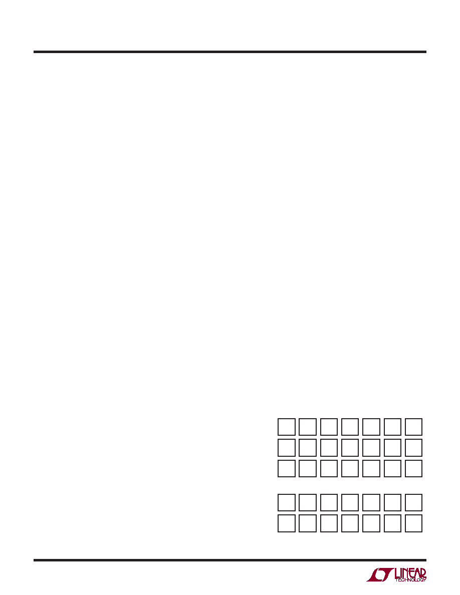
block diagram in Figure 10.
Figure 10. Sequencer Memory Block Diagram
LOCATION 0000
DIFF
A2
A1
A0
UNI/BIP
PGA
EOS
LOCATION 0001
LOCATION 0010
LOCATION 1110
LOCATION 1111
18523 F10
APPLICATIONS INFORMATION
相关PDF资料 |
PDF描述 |
|---|---|
| MS27473E8A6SA | CONN PLUG 6POS STRAIGHT W/SCKT |
| VE-B53-MW-S | CONVERTER MOD DC/DC 24V 100W |
| D38999/20MG75BA | CONN HSG RCPT 4POS WALL MT SCKT |
| LTC1298IN8#PBF | IC A/D CONV SAMPLING 12BIT 8-DIP |
| VE-232-MY | CONVERTER MOD DC/DC 15V 50W |
相关代理商/技术参数 |
参数描述 |
|---|---|
| LTC1852IFW | 功能描述:IC A/D CONV 8CH 10BIT 48-TSSOP RoHS:否 类别:集成电路 (IC) >> 数据采集 - 模数转换器 系列:- 标准包装:1,000 系列:- 位数:16 采样率(每秒):45k 数据接口:串行 转换器数目:2 功率耗散(最大):315mW 电压电源:模拟和数字 工作温度:0°C ~ 70°C 安装类型:表面贴装 封装/外壳:28-SOIC(0.295",7.50mm 宽) 供应商设备封装:28-SOIC W 包装:带卷 (TR) 输入数目和类型:2 个单端,单极 |
| LTC1852IFW#PBF | 功能描述:IC A/D CONV 8CH 10BIT 48-TSSOP RoHS:是 类别:集成电路 (IC) >> 数据采集 - 模数转换器 系列:- 标准包装:1,000 系列:- 位数:16 采样率(每秒):45k 数据接口:串行 转换器数目:2 功率耗散(最大):315mW 电压电源:模拟和数字 工作温度:0°C ~ 70°C 安装类型:表面贴装 封装/外壳:28-SOIC(0.295",7.50mm 宽) 供应商设备封装:28-SOIC W 包装:带卷 (TR) 输入数目和类型:2 个单端,单极 |
| LTC1852IFW#TR | 功能描述:IC A/D CONV 8CH 10BIT 48-TSSOP RoHS:否 类别:集成电路 (IC) >> 数据采集 - 模数转换器 系列:- 标准包装:1,000 系列:- 位数:16 采样率(每秒):45k 数据接口:串行 转换器数目:2 功率耗散(最大):315mW 电压电源:模拟和数字 工作温度:0°C ~ 70°C 安装类型:表面贴装 封装/外壳:28-SOIC(0.295",7.50mm 宽) 供应商设备封装:28-SOIC W 包装:带卷 (TR) 输入数目和类型:2 个单端,单极 |
| LTC1852IFW#TRPBF | 功能描述:IC A/D CONV 8CH 10BIT 48-TSSOP RoHS:是 类别:集成电路 (IC) >> 数据采集 - 模数转换器 系列:- 标准包装:1,000 系列:- 位数:16 采样率(每秒):45k 数据接口:串行 转换器数目:2 功率耗散(最大):315mW 电压电源:模拟和数字 工作温度:0°C ~ 70°C 安装类型:表面贴装 封装/外壳:28-SOIC(0.295",7.50mm 宽) 供应商设备封装:28-SOIC W 包装:带卷 (TR) 输入数目和类型:2 个单端,单极 |
| LTC1853CFW | 功能描述:IC A/D CONV 8CH 12BIT 48-TSSOP RoHS:否 类别:集成电路 (IC) >> 数据采集 - 模数转换器 系列:- 标准包装:1,000 系列:- 位数:16 采样率(每秒):45k 数据接口:串行 转换器数目:2 功率耗散(最大):315mW 电压电源:模拟和数字 工作温度:0°C ~ 70°C 安装类型:表面贴装 封装/外壳:28-SOIC(0.295",7.50mm 宽) 供应商设备封装:28-SOIC W 包装:带卷 (TR) 输入数目和类型:2 个单端,单极 |
发布紧急采购,3分钟左右您将得到回复。