- 您现在的位置:买卖IC网 > PDF目录10273 > LTC1852IFW#TR (Linear Technology)IC A/D CONV 8CH 10BIT 48-TSSOP PDF资料下载
参数资料
| 型号: | LTC1852IFW#TR |
| 厂商: | Linear Technology |
| 文件页数: | 5/24页 |
| 文件大小: | 0K |
| 描述: | IC A/D CONV 8CH 10BIT 48-TSSOP |
| 标准包装: | 1,800 |
| 位数: | 10 |
| 采样率(每秒): | 400k |
| 数据接口: | 并联 |
| 转换器数目: | 1 |
| 功率耗散(最大): | 15mW |
| 电压电源: | 单电源 |
| 工作温度: | -40°C ~ 85°C |
| 安装类型: | 表面贴装 |
| 封装/外壳: | 48-TFSOP(0.240",6.10mm 宽) |
| 供应商设备封装: | 48-TSSOP |
| 包装: | 带卷 (TR) |
| 输入数目和类型: | 8 个单端,单极;8 个单端,双极;4 个差分,单极;4 个差分,双极 |
| 其它名称: | LTC1852IFWTR |
LTC1852/LTC1853
13
18523fa
LT1809/LT1810: Single and Dual 180MHz Rail-to-Rail
Voltage Feedback Amplier. Single 3V to ±15V supplies.
20mA supply current. Lowest distortion.
LT1812/LT1813: Single and Dual 100MHz Voltage Feed-
back Amplier. Single 5V to ±5V supplies. 3.6mA supply
current. Low noise and low distortion.
Input Filtering
The noise and the distortion of the input amplier and
other circuitry must be considered since they will add to
the LTC1852/LTC1853 noise and distortion. Noisy input
circuitry should be ltered prior to the analog inputs to
minimize noise. A simple 1-pole RC lter is sufcient for
many applications. For instance, a 200Ω source resistor
and a 1000pF capacitor to ground on the input will limit
the input bandwidth to 800kHz.The capacitor also acts
as a charge reservoir for the input sample-and-hold and
isolates the ADC input from sampling glitch sensitive
circuitry. High quality capacitors and resistors should be
used since these components can add distortion. NPO
and silver mica type dielectric capacitors have excellent
linearity.Carbon surface mount resistors can also generate
distortion from self heating and from damage that may
occur during soldering.Metal lm surface mount resistors
are much less susceptible to both problems.
REFERENCE
The LTC1852/LTC1853 includes an on-chip, temperature
compensated, curvature corrected, bandgap reference
that is factory trimmed to 2.500V and has a very exible
3-pin interface. REFOUT is the 2.5V bandgap output, REFIN
is the input to the reference buffer and REFCOMP is the
reference buffer output. The input span is determined by
the voltage appearing on the REFCOMP pin as shown in
Table 2. The reference buffer has a gain of 1.6384 and
is factory trimmed by forcing an external 2.500V on the
REFIN pin and trimming REFCOMP to 4.096V. The 3-pin
interface allows for three pin-strappable Reference modes
as well as two additional external Reference modes. For
voltages on the REFIN pin ranging from 1V to 2.6V, the
output voltage on REFCOMP will equal 1.6384 times the
voltage on the REFIN pin. In this mode, the REFIN pin can
be tied to REFOUT to use the internal 2.5V reference to get
4.096V on REFCOMP or driven with an external reference
or DAC. If REFIN is tied low, the internal 2.5V reference
divided by 2 (1.25V) is connected internally to the input
of the reference buffer resulting in 2.048V on REFCOMP.
If REFIN is tied high, the reference buffer is disabled and
REFCOMP can be tied to REFOUT to achieve a 2.5V span
or driven with an external reference or DAC. Table 3 sum-
marizes the Reference modes.
Table 3. Reference Mode Table
MODE
REFIN
REFCOMP
REFIN Tied Low
0V Input
2.048V Output
REFIN is Buffer Input
1v to 2.6 Input
1.6384V to 4.26V Output
(1.6384 REFIN)
REFIN Tied High
5V Input
Input, 19.2kΩ to Ground
Full Scale and Offset
In applications where absolute accuracy is important,
offset and full-scale errors can be adjusted to zero dur-
ing a calibration sequence. Offset error must be adjusted
before full-scale error. Zero offset is achieved by adjust-
ing the offset applied to the “–” input. For single-ended
inputs, this offset should be applied to the COM pin. For
differential inputs, the “–” input is dictated by the MUX
address. For zero offset error, apply 0.5LSB (actual volt-
age will vary with input span selected) to the “+” input
and adjust the offset at the “–” input until the output code
ickers between 0000 0000 0000 and 0000 0000 0001
for the LTC1853 and between 00 0000 0000 and 00 0000
0001 for the LTC1852.
As mentioned earlier, the internal reference is factory
trimmed to 2.500V. To make sure that the reference buffer
gain is not compensating for trim errors in the reference,
REFCOMP is trimmed to 4.096V with an extremely accurate
external 2.5V reference applied to REFIN. Likewise, to make
sure that the full-scale gain trim is not compensating for
errors in the reference buffer gain, the input full-scale gain
is trimmed with an extremely accurate 4.096V reference
applied to REFCOMP (REFIN = 5V to disable the reference
buffer). This allows the use of either a 2.5V reference applied
to REFIN or a 4.096V reference applied to REFCOMP to
achieve accurate results. Full-scale errors can be trimmed
to zero by adjusting the appropriate reference voltage. For
unipolar inputs, an input voltage of FS – 1.5LSBs should
be applied to the “+” input and the appropriate reference
APPLICATIONS INFORMATION
相关PDF资料 |
PDF描述 |
|---|---|
| D38999/20JJ24PNLC | CONN HSG RCPT 24POS WALL MT PINS |
| LTC2449CUHF | IC ADC 24BIT HI SPEED 38QFN |
| VI-212-MX-S | CONVERTER MOD DC/DC 15V 75W |
| MS27497E16F99P | CONN RCPT 23POS WALL MNT W/PINS |
| VI-2NW-MY | CONVERTER MOD DC/DC 5.5V 50W |
相关代理商/技术参数 |
参数描述 |
|---|---|
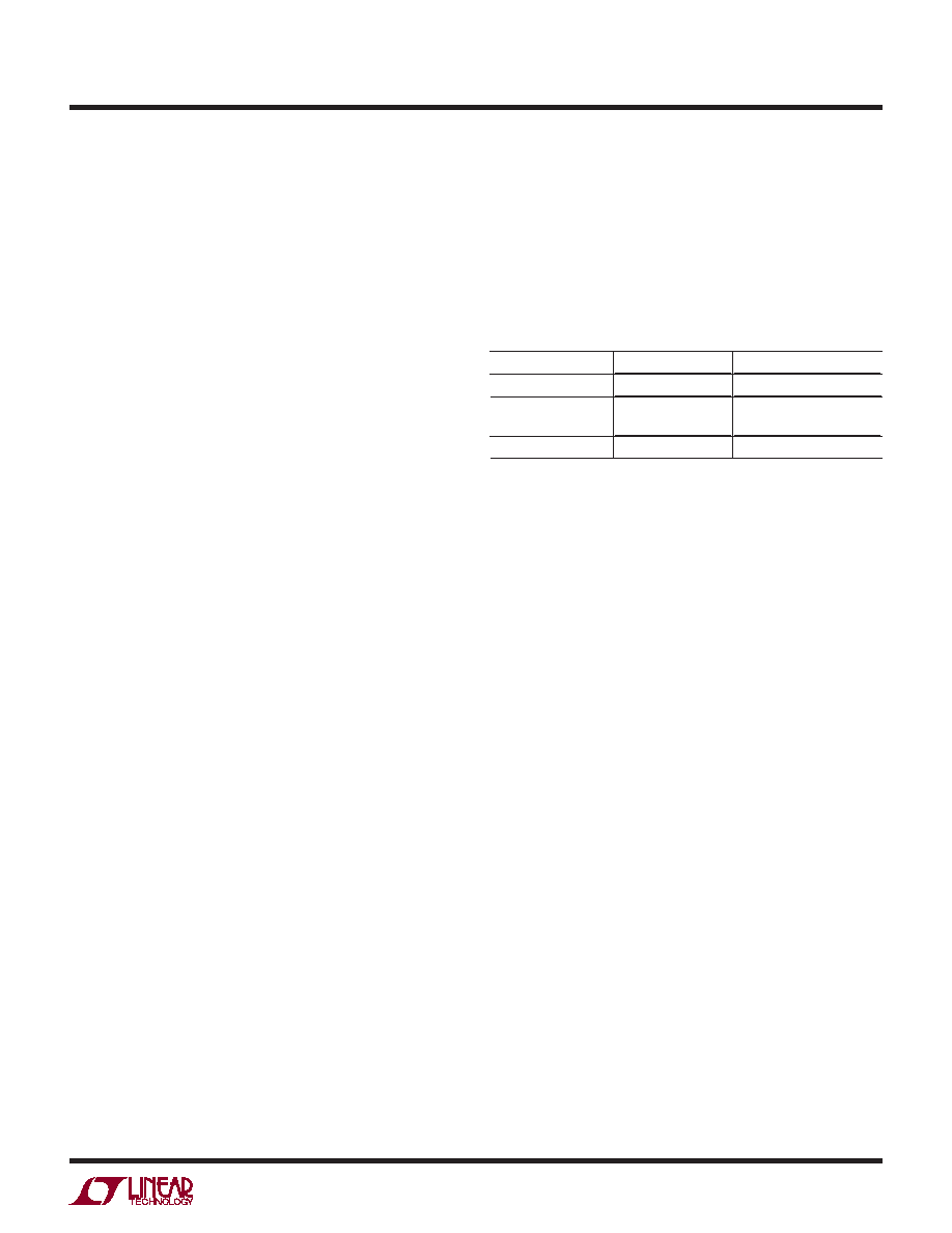
| LTC1853CFW | 功能描述:IC A/D CONV 8CH 12BIT 48-TSSOP RoHS:否 类别:集成电路 (IC) >> 数据采集 - 模数转换器 系列:- 标准包装:1,000 系列:- 位数:16 采样率(每秒):45k 数据接口:串行 转换器数目:2 功率耗散(最大):315mW 电压电源:模拟和数字 工作温度:0°C ~ 70°C 安装类型:表面贴装 封装/外壳:28-SOIC(0.295",7.50mm 宽) 供应商设备封装:28-SOIC W 包装:带卷 (TR) 输入数目和类型:2 个单端,单极 |
| LTC1853CFW#PBF | 功能描述:IC A/D CONV 8CH 12BIT 48-TSSOP RoHS:是 类别:集成电路 (IC) >> 数据采集 - 模数转换器 系列:- 标准包装:1 系列:microPOWER™ 位数:8 采样率(每秒):1M 数据接口:串行,SPI? 转换器数目:1 功率耗散(最大):- 电压电源:模拟和数字 工作温度:-40°C ~ 125°C 安装类型:表面贴装 封装/外壳:24-VFQFN 裸露焊盘 供应商设备封装:24-VQFN 裸露焊盘(4x4) 包装:Digi-Reel® 输入数目和类型:8 个单端,单极 产品目录页面:892 (CN2011-ZH PDF) 其它名称:296-25851-6 |
| LTC1853CFW#TR | 功能描述:IC A/D CONV 8CH 12BIT 48-TSSOP RoHS:否 类别:集成电路 (IC) >> 数据采集 - 模数转换器 系列:- 标准包装:1,000 系列:- 位数:16 采样率(每秒):45k 数据接口:串行 转换器数目:2 功率耗散(最大):315mW 电压电源:模拟和数字 工作温度:0°C ~ 70°C 安装类型:表面贴装 封装/外壳:28-SOIC(0.295",7.50mm 宽) 供应商设备封装:28-SOIC W 包装:带卷 (TR) 输入数目和类型:2 个单端,单极 |
| LTC1853CFW#TRPBF | 功能描述:IC A/D CONV 8CH 12BIT 48-TSSOP RoHS:是 类别:集成电路 (IC) >> 数据采集 - 模数转换器 系列:- 标准包装:1,000 系列:- 位数:16 采样率(每秒):45k 数据接口:串行 转换器数目:2 功率耗散(最大):315mW 电压电源:模拟和数字 工作温度:0°C ~ 70°C 安装类型:表面贴装 封装/外壳:28-SOIC(0.295",7.50mm 宽) 供应商设备封装:28-SOIC W 包装:带卷 (TR) 输入数目和类型:2 个单端,单极 |
| LTC1853IFW | 功能描述:IC A/D CONV 8CH 12BIT 48-TSSOP RoHS:否 类别:集成电路 (IC) >> 数据采集 - 模数转换器 系列:- 标准包装:1,000 系列:- 位数:12 采样率(每秒):300k 数据接口:并联 转换器数目:1 功率耗散(最大):75mW 电压电源:单电源 工作温度:0°C ~ 70°C 安装类型:表面贴装 封装/外壳:24-SOIC(0.295",7.50mm 宽) 供应商设备封装:24-SOIC 包装:带卷 (TR) 输入数目和类型:1 个单端,单极;1 个单端,双极 |
发布紧急采购,3分钟左右您将得到回复。