- 您现在的位置:买卖IC网 > PDF目录10250 > LTC1853IFW#TR (Linear Technology)IC A/D CONV 8CH 12BIT 48-TSSOP PDF资料下载
参数资料
| 型号: | LTC1853IFW#TR |
| 厂商: | Linear Technology |
| 文件页数: | 7/24页 |
| 文件大小: | 0K |
| 描述: | IC A/D CONV 8CH 12BIT 48-TSSOP |
| 标准包装: | 1,800 |
| 位数: | 12 |
| 采样率(每秒): | 400k |
| 数据接口: | 并联 |
| 转换器数目: | 1 |
| 功率耗散(最大): | 15mW |
| 电压电源: | 单电源 |
| 工作温度: | -40°C ~ 85°C |
| 安装类型: | 表面贴装 |
| 封装/外壳: | 48-TFSOP(0.240",6.10mm 宽) |
| 供应商设备封装: | 48-TSSOP |
| 包装: | 带卷 (TR) |
| 输入数目和类型: | 8 个单端,单极;8 个单端,双极;4 个差分,单极;4 个差分,双极 |
| 其它名称: | LTC1853IFWTR |
LTC1852/LTC1853
15
18523fa
BOARD LAYOUT AND BYPASSING
To obtain the best performance from the LTC1852/LTC1853,
a printed circuit board with ground plane is required. The
ground plane under the ADC area should be as free of
breaks and holes as possible, such that a low impedance
path between all ADC grounds and all ADC decoupling
capacitors is provided. It is critical to prevent digital noise
from being coupled to the analog inputs, reference or
analog power supply lines. Layout for the printed circuit
board should ensure that digital and analog signal lines are
separated as much as possible. In particular, care should
be taken not to run any digital track alongside an analog
signal track or underneath the ADC.
An analog ground plane separate from the logic system
ground should be established under and around the ADC.
Pin 34 (OGND), Pin 13 (GND), Pin 16 (GND) and all other
analog grounds should be connected to this single ana-
log ground point. The bypass capacitors should also be
connected to this analog ground plane. No other digital
grounds should be connected to this analog ground plane.
In some applications, it may be desirable to connect the
OVDD to the logic system supply and OGND to the logic
system ground. In these cases, OVDD should be bypassed
to OGND instead of the analog ground plane.
Low impedance analog and digital power supply common
returns are essential to the low noise operation of the
ADC and the foil width for these tracks should be as wide
as possible. In applications where the ADC data outputs
and control signals are connected to a continuously ac-
tive microprocessor bus, it is possible to get errors in the
conversion results. These errors are due to feedthrough
from the microprocessor to the sucessive approximation
comparator. The problem can be eliminated by forcing the
microprocessor into a WAIT state during conversions or
by using three-state buffers to isolate the ADC bus. The
traces connecting the pins and bypass capacitors must be
kept short and should be made as wide as possible.
The LTC1852/LTC1853 have differential inputs to mini-
mize noise coupling. Common mode noise on the “+”
and “–” inputs will be rejected by the input CMRR. The
LTC1852/LTC1853 will hold and convert the difference
between whichever input is selected as the “+” input and
whichever input is selected as the “–” input. Leads to the
inputs should be kept as short as possible.
SUPPLY BYPASSING
High quality, low series resistance ceramic 10μF bypass
capacitors should be used. Surface mount ceramic ca-
pacitors such as Murata GRM235Y5V106Z016 provide
excellent bypassing in a small board space. Alternatively,
10μF tantalum capacitors in parallel with 0.1μF ceramic
capacitors can be used. Bypass capacitors must be located
as close to the pins as possible. The traces connecting the
pins and the bypass capacitors must be kept short and
should be made as wide as possible.
DIGITAL INTERFACE
Internal Clock
The A/D converter has an internal clock that eliminates the
need of synchronization between the external clock and
the CS and RD signals found in other ADCs. The internal
clock is factory trimmed to achieve a typical conversion
time of 1400ns, and a maximum conversion time over
the full operating temperature range of 2μs. No external
adjustments are required. The guaranteed maximum
acquisition time is 150ns. In addition, a throughput
time of 2.5μs and a minimum sampling rate of 400ksps
is guaranteed.
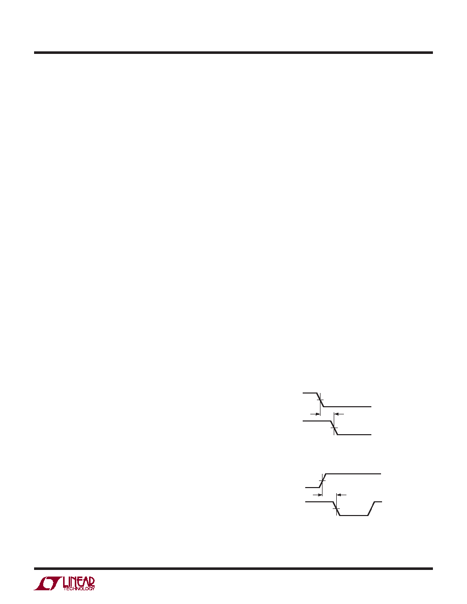
SHDN
CONVST
t4
18523 F03
CS
SHDN
t3
18523 F02
Figure 3. SHDN to CONVST Wake-Up Timing
Figure 2. CS to SHDN Setup Timing
APPLICATIONS INFORMATION
相关PDF资料 |
PDF描述 |
|---|---|
| VE-233-CU-F1 | CONVERTER MOD DC/DC 24V 200W |
| AD7651ASTZRL | IC ADC 16BIT UNIPOLAR 48LFCSP |
| AD7651ACPZRL | IC ADC 16BIT UNIPOLAR 48LQFP |
| CS5532-BSZR | IC ADC 24BIT 2CH W/LNA 20-SSOP |
| LTC1851IFW#PBF | IC ADC 12BIT 1.25MSPS 48-TSSOP |
相关代理商/技术参数 |
参数描述 |
|---|---|
| LTC1854CG#PBF | 功能描述:IC ADC 12BIT 8CH 100KSPS 28SSOP RoHS:是 类别:集成电路 (IC) >> 数据采集 - 模数转换器 系列:- 标准包装:1,000 系列:- 位数:16 采样率(每秒):45k 数据接口:串行 转换器数目:2 功率耗散(最大):315mW 电压电源:模拟和数字 工作温度:0°C ~ 70°C 安装类型:表面贴装 封装/外壳:28-SOIC(0.295",7.50mm 宽) 供应商设备封装:28-SOIC W 包装:带卷 (TR) 输入数目和类型:2 个单端,单极 |
| LTC1854CG#TRPBF | 功能描述:IC ADC 12BIT 8CH 100KSPS 28SSOP RoHS:是 类别:集成电路 (IC) >> 数据采集 - 模数转换器 系列:- 标准包装:1,000 系列:- 位数:16 采样率(每秒):45k 数据接口:串行 转换器数目:2 功率耗散(最大):315mW 电压电源:模拟和数字 工作温度:0°C ~ 70°C 安装类型:表面贴装 封装/外壳:28-SOIC(0.295",7.50mm 宽) 供应商设备封装:28-SOIC W 包装:带卷 (TR) 输入数目和类型:2 个单端,单极 |
| LTC1854IG#PBF | 功能描述:IC ADC 12BIT 8CH 100KSPS 28SSOP RoHS:是 类别:集成电路 (IC) >> 数据采集 - 模数转换器 系列:- 标准包装:1,000 系列:- 位数:12 采样率(每秒):300k 数据接口:并联 转换器数目:1 功率耗散(最大):75mW 电压电源:单电源 工作温度:0°C ~ 70°C 安装类型:表面贴装 封装/外壳:24-SOIC(0.295",7.50mm 宽) 供应商设备封装:24-SOIC 包装:带卷 (TR) 输入数目和类型:1 个单端,单极;1 个单端,双极 |
| LTC1854IG#TRPBF | 功能描述:IC ADC 12BIT 8CH 100KSPS 28SSOP RoHS:是 类别:集成电路 (IC) >> 数据采集 - 模数转换器 系列:- 标准包装:1,000 系列:- 位数:16 采样率(每秒):45k 数据接口:串行 转换器数目:2 功率耗散(最大):315mW 电压电源:模拟和数字 工作温度:0°C ~ 70°C 安装类型:表面贴装 封装/外壳:28-SOIC(0.295",7.50mm 宽) 供应商设备封装:28-SOIC W 包装:带卷 (TR) 输入数目和类型:2 个单端,单极 |
| LTC1855CG#PBF | 功能描述:IC ADC 14BIT 8CH 100KSPS 28SSOP RoHS:是 类别:集成电路 (IC) >> 数据采集 - 模数转换器 系列:- 标准包装:1,000 系列:- 位数:12 采样率(每秒):300k 数据接口:并联 转换器数目:1 功率耗散(最大):75mW 电压电源:单电源 工作温度:0°C ~ 70°C 安装类型:表面贴装 封装/外壳:24-SOIC(0.295",7.50mm 宽) 供应商设备封装:24-SOIC 包装:带卷 (TR) 输入数目和类型:1 个单端,单极;1 个单端,双极 |
发布紧急采购,3分钟左右您将得到回复。