- 您现在的位置:买卖IC网 > PDF目录2005 > LTC1853IFW#TRPBF (Linear Technology)IC A/D CONV 8CH 12BIT 48-TSSOP PDF资料下载
参数资料
| 型号: | LTC1853IFW#TRPBF |
| 厂商: | Linear Technology |
| 文件页数: | 2/24页 |
| 文件大小: | 0K |
| 描述: | IC A/D CONV 8CH 12BIT 48-TSSOP |
| 标准包装: | 1,800 |
| 位数: | 12 |
| 采样率(每秒): | 400k |
| 数据接口: | 并联 |
| 转换器数目: | 1 |
| 功率耗散(最大): | 15mW |
| 电压电源: | 单电源 |
| 工作温度: | -40°C ~ 85°C |
| 安装类型: | 表面贴装 |
| 封装/外壳: | 48-TFSOP(0.240",6.10mm 宽) |
| 供应商设备封装: | 48-TSSOP |
| 包装: | 带卷 (TR) |
| 输入数目和类型: | 8 个单端,单极;8 个单端,双极;4 个差分,单极;4 个差分,双极 |
LTC1852/LTC1853
10
18523fa
The LTC1852/LTC1853 are complete and very exible
data acquisition systems. They consist of a 10-bit/12-bit,
400ksps capacitive successive approximation A/D con-
verter with a wideband sample-and-hold, a congurable
8-channel analog input multiplexer, an internal reference
and reference buffer amplier, a 16-bit parallel digital
output and digital control logic, including a programmable
sequencer.
CONVERSION DETAILS
The core analog-to-digital converter in the LTC1852/
LTC1853 uses a successive approximation algorithm and
an internal sample-and-hold circuit to convert an analog
signal to a 10-bit/12-bit parallel output. Conversion start
is controlled by the CS and CONVST inputs. At the start
of the conversion, the successive approximation register
(SAR) is reset. Once a conversion cycle is begun, it cannot
be restarted. During the conversion, the internal differen-
tial capacitive DAC output is sequenced by the SAR from
the most signicant bit (MSB) to the least signicant bit
(LSB). The outputs of the analog input multiplexer are
connected to the sample-and-hold capacitors (CSAMPLE)
during the acquire phase and the comparator offset is
nulled by the zeroing switches. In this acquire phase, a
minimum delay of 150ns will provide enough time for
the sample-and-hold capacitors to acquire the analog
signal. During the convert phase, the comparator zeroing
switches are open, putting the comparator into compare
mode. The input switches connect CSAMPLE to ground,
transferring the differential analog input charge onto the
summing junction. This input charge is successively
compared with the binary weighted charges supplied by
the differential capacitive DAC. Bit decisions are made by
the high speed comparator. At the end of the conversion,
the differential DAC output balances the input charges.
The SAR contents (a 10-bit/12-bit data word), which
represents the difference of the analog input multiplexer
outputs, and the 4-bit address word are loaded into the
14-bit/16-bit output latches.
DYNAMIC PERFORMANCE
Signal-to-(Noise + Distortion) Ratio
The signal-to-noise plus distortion ratio [S/(N + D)] is the
ratio between the RMS amplitude of the fundamental input
frequency and the RMS amplitude of all other frequency
components at the ADC output. The output is band lim-
ited to frequencies above DC to below half the sampling
frequency. The effective number of bits (ENOBs) is a
measurement of the resolution of an ADC and is directly
related to the S/(N + D) by the equation:
ENOB = [S/(N + D) – 1.76]/6.02
where ENOB is the effective number of bits and S/(N + D) is
expressed in dB. At the maximum sampling rate of 400kHz,
the LTC1852/LTC1853 maintain near ideal ENOBs up to
and beyond the Nyquist input frequency of 200kHz.
Total Harmonic Distortion
Total harmonic distortion is the ratio of the RMS sum
of all harmonics of the input signal to the fundamental
itself. The out-of-band harmonics alias into the frequency
band between DC and half the sampling frequency. THD
is expressed as:
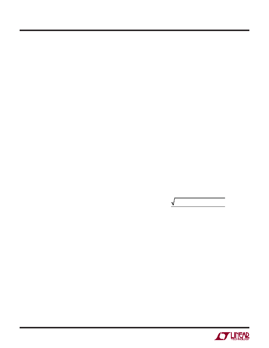
THD = 20Log
V2
2 + V32 + V42 +...Vn2
V1
where V1 is the RMS amplitude of the fundamental
frequency and V2 through Vn are the amplitudes of the
second through nth harmonics. The LTC1852/LTC1853
have good distortion performance up to the Nyquist
frequency and beyond.
Intermodulation Distortion
If the ADC input signal consists of more than one spectral
component, the ADC transfer function nonlinearity can
produce intermodulation distortion (IMD) in addition to
THD. IMD is the change in one sinusoidal input caused
by the presence of another sinusoidal input at a different
frequency.
APPLICATIONS INFORMATION
相关PDF资料 |
PDF描述 |
|---|---|
| LTC1856IG#PBF | IC ADC 16BIT 100KSPS 28-SSOP |
| LTC1859IG#TRPBF | IC A/D CONV 8CH 16BIT 28-SSOP |
| LTC1867AIGN#TRPBF | IC ADC 16BIT 8CH 200KSPS 16SSOP |
| LTC1867LCGN#PBF | IC ADC 16BIT 8CH 175KSPS 16SSOP |
| LTC2142IUP-14#PBF | IC ADC DUAL 14BIT 65MSPS 64QFN |
相关代理商/技术参数 |
参数描述 |
|---|---|
| LTC1854CG#PBF | 功能描述:IC ADC 12BIT 8CH 100KSPS 28SSOP RoHS:是 类别:集成电路 (IC) >> 数据采集 - 模数转换器 系列:- 标准包装:1,000 系列:- 位数:16 采样率(每秒):45k 数据接口:串行 转换器数目:2 功率耗散(最大):315mW 电压电源:模拟和数字 工作温度:0°C ~ 70°C 安装类型:表面贴装 封装/外壳:28-SOIC(0.295",7.50mm 宽) 供应商设备封装:28-SOIC W 包装:带卷 (TR) 输入数目和类型:2 个单端,单极 |
| LTC1854CG#TRPBF | 功能描述:IC ADC 12BIT 8CH 100KSPS 28SSOP RoHS:是 类别:集成电路 (IC) >> 数据采集 - 模数转换器 系列:- 标准包装:1,000 系列:- 位数:16 采样率(每秒):45k 数据接口:串行 转换器数目:2 功率耗散(最大):315mW 电压电源:模拟和数字 工作温度:0°C ~ 70°C 安装类型:表面贴装 封装/外壳:28-SOIC(0.295",7.50mm 宽) 供应商设备封装:28-SOIC W 包装:带卷 (TR) 输入数目和类型:2 个单端,单极 |
| LTC1854IG#PBF | 功能描述:IC ADC 12BIT 8CH 100KSPS 28SSOP RoHS:是 类别:集成电路 (IC) >> 数据采集 - 模数转换器 系列:- 标准包装:1,000 系列:- 位数:12 采样率(每秒):300k 数据接口:并联 转换器数目:1 功率耗散(最大):75mW 电压电源:单电源 工作温度:0°C ~ 70°C 安装类型:表面贴装 封装/外壳:24-SOIC(0.295",7.50mm 宽) 供应商设备封装:24-SOIC 包装:带卷 (TR) 输入数目和类型:1 个单端,单极;1 个单端,双极 |
| LTC1854IG#TRPBF | 功能描述:IC ADC 12BIT 8CH 100KSPS 28SSOP RoHS:是 类别:集成电路 (IC) >> 数据采集 - 模数转换器 系列:- 标准包装:1,000 系列:- 位数:16 采样率(每秒):45k 数据接口:串行 转换器数目:2 功率耗散(最大):315mW 电压电源:模拟和数字 工作温度:0°C ~ 70°C 安装类型:表面贴装 封装/外壳:28-SOIC(0.295",7.50mm 宽) 供应商设备封装:28-SOIC W 包装:带卷 (TR) 输入数目和类型:2 个单端,单极 |
| LTC1855CG#PBF | 功能描述:IC ADC 14BIT 8CH 100KSPS 28SSOP RoHS:是 类别:集成电路 (IC) >> 数据采集 - 模数转换器 系列:- 标准包装:1,000 系列:- 位数:12 采样率(每秒):300k 数据接口:并联 转换器数目:1 功率耗散(最大):75mW 电压电源:单电源 工作温度:0°C ~ 70°C 安装类型:表面贴装 封装/外壳:24-SOIC(0.295",7.50mm 宽) 供应商设备封装:24-SOIC 包装:带卷 (TR) 输入数目和类型:1 个单端,单极;1 个单端,双极 |
发布紧急采购,3分钟左右您将得到回复。