- 您现在的位置:买卖IC网 > PDF目录10661 > LTC1858CG#PBF (Linear Technology)IC ADC 8CH 14BIT 100KSPS 28-SSOP PDF资料下载
参数资料
| 型号: | LTC1858CG#PBF |
| 厂商: | Linear Technology |
| 文件页数: | 5/20页 |
| 文件大小: | 0K |
| 描述: | IC ADC 8CH 14BIT 100KSPS 28-SSOP |
| 标准包装: | 47 |
| 系列: | SoftSpan™ |
| 位数: | 14 |
| 采样率(每秒): | 100k |
| 数据接口: | MICROWIRE?,串行,SPI? |
| 转换器数目: | 1 |
| 功率耗散(最大): | 40mW |
| 电压电源: | 模拟和数字 |
| 工作温度: | 0°C ~ 70°C |
| 安装类型: | 表面贴装 |
| 封装/外壳: | 28-SSOP(0.209",5.30mm 宽) |
| 供应商设备封装: | 28-SSOP |
| 包装: | 管件 |
| 输入数目和类型: | 8 个单端,单极;8 个单端,双极;4 个差分,单极;4 个差分,双极 |
| 产品目录页面: | 1347 (CN2011-ZH PDF) |
LTC1857/LTC1858/LTC1859
13
185789fa
APPLICATIONS INFORMATION
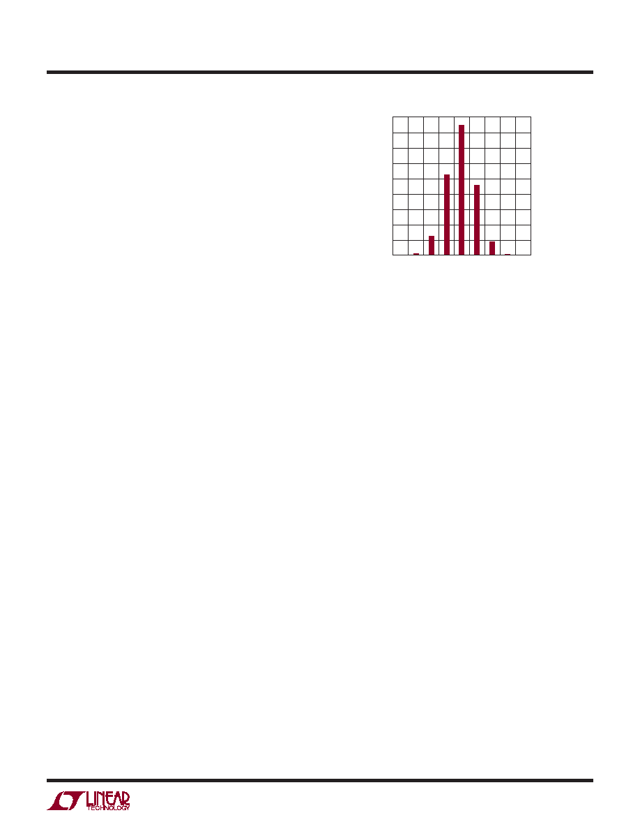
Figure 5. LTC1859 Histogram for 4096 Conversions
11 1111 1111 1111 for the LTC1858 and between 0000
0000 0000 and 1111 1111 1111 for the LTC1857.
As mentioned earlier, the internal reference is factory
trimmed to 2.50V. To make sure that the reference buffer
gain is not compensating for trim errors in the reference,
REFCOMP is trimmed with an accurate external 2.5V refer-
ence applied to VREF. For unipolar inputs, an input voltage
of FS – 1.5LSBs should be applied to the “+” input and the
appropriate reference adjusted until the output code ick-
ers between 1111 1111 1111 1110 and 1111 1111 1111
1111 for the LTC1859, between 11 1111 1111 1110 and
11 1111 1111 1111 for the LTC1858 and between 1111
1111 1110 and 1111 1111 1111 for the LTC1857.
For bipolar inputs, an input voltage of FS – 1.5LSBs should
be applied to the “+” input and the appropriate reference
adjusted until the output code ickers between 0111 1111
1111 1110 and 0111 1111 1111 1111 for the LTC1859,
between 01 1111 1111 1110 and 01 1111 1111 1111 for
the LTC1858 and between 0111 1111 1110 and 0111 1111
1111 for the LTC1857.
These adjustments as well as the factory trims affect all
channels. The channel-to-channel offset and gain error
matching are guaranteed by design to meet the specica-
tions in the Converter Characteristics table.
DC PERFORMANCE
One way of measuring the transition noise associated
with a high resolution ADC is to use a technique where
a DC signal is applied to the input of the MUX and the
resulting output codes are collected over a large number
of conversions. For example in Figure 5 the distribution
of output code is shown for a DC input that has been
digitized 4096 times. The distribution is Gaussian and the
RMS code transition is about 1LSB for the LTC1859.
DIGITAL INTERFACE
Internal Clock
The ADC has an internal clock that is trimmed to achieve
a typical conversion time of 4μs. No external adjustments
are required and, with the maximum acquisition time of
4μs, throughput performance of 100ksps is assured.
3V Input/Output Compatible
The LTC1857/LTC1858/LTC1859 operate on a 5V supply,
which makes the devices easy to interface to 5V digital
systems. These devices can also interface to 3V digital
systems: the digital input pins (SCK, SDI, CONVST and
RD) of the LTC1857/LTC1858/LTC1859 recognize 3V or 5V
inputs. The LTC1857/LTC1858/LTC1859 have a dedicated
output supply pin (OVP) that controls the output swings
of the digital output pins (SDO, BUSY) and allows the part
to interface to either 3V or 5V digital systems. The output
is two’s complement binary for bipolar mode and offset
binary for unipolar mode.
Timing and Control
Conversion start and data read are controlled by two digital
inputs: CONVST and RD. To start a conversion and put
the sample-and-hold into the hold mode bring CONVST
high for no less than 40ns. Once initiated it cannot be re-
started until the conversion is complete. Converter status
is indicated by the BUSY output and this is low while the
conversion is in progress.
Figures 6a and 6b show two different modes of opera-
tion for the LTC1859. For the 12-bit LTC1857 and 14-bit
LTC1858, the last four and two bits of the SDO will output
zeros respectively. In mode 1 (Figure 6a), RD is tied low.
The rising edge of CONVST starts the conversion. The data
outputs are always enabled. The MSB of the data output
is available after the conversion. In mode 2 (Figure 6b),
CONVST and RD are tied together. The rising edge of the
CONVST signal starts the conversion. Data outputs are in
CODE
–4
–3
0
COUNT
200
600
800
1000
23
1800
1859 F05
400
–2
–1
0
14
1200
1400
1600
相关PDF资料 |
PDF描述 |
|---|---|
| MAX972CSA+T | IC COMPARATOR OD 8-SOIC |
| VI-B1V-IV-F4 | CONVERTER MOD DC/DC 5.8V 150W |
| MAX9041BESA+ | IC COMPARATOR SNGL 8-SOIC |
| LTC1273BCSW#PBF | IC A/D CONV 12BIT SAMPLNG 24SOIC |
| MAX972EBL+T | IC COMPARATOR OPN DRN DL 9UCSP |
相关代理商/技术参数 |
参数描述 |
|---|---|
| LTC1858IG#PBF | 功能描述:IC A/D CONV 8CH 14BIT 28-SSOP RoHS:是 类别:集成电路 (IC) >> 数据采集 - 模数转换器 系列:SoftSpan™ 标准包装:1 系列:- 位数:14 采样率(每秒):83k 数据接口:串行,并联 转换器数目:1 功率耗散(最大):95mW 电压电源:双 ± 工作温度:0°C ~ 70°C 安装类型:通孔 封装/外壳:28-DIP(0.600",15.24mm) 供应商设备封装:28-PDIP 包装:管件 输入数目和类型:1 个单端,双极 |
| LTC1858IG#TRPBF | 功能描述:IC A/D CONV 8CH 14BIT 28-SSOP RoHS:是 类别:集成电路 (IC) >> 数据采集 - 模数转换器 系列:SoftSpan™ 标准包装:1,000 系列:- 位数:12 采样率(每秒):300k 数据接口:并联 转换器数目:1 功率耗散(最大):75mW 电压电源:单电源 工作温度:0°C ~ 70°C 安装类型:表面贴装 封装/外壳:24-SOIC(0.295",7.50mm 宽) 供应商设备封装:24-SOIC 包装:带卷 (TR) 输入数目和类型:1 个单端,单极;1 个单端,双极 |
| LTC1859CG | 制造商:Linear Technology 功能描述:ADC Single SAR 100ksps 16-bit Serial 28-Pin SSOP |
| LTC1859CG#PBF | 功能描述:IC ADC 8CH 16BIT 100KSPS 28-SSOP RoHS:是 类别:集成电路 (IC) >> 数据采集 - 模数转换器 系列:SoftSpan™ 标准包装:1 系列:microPOWER™ 位数:8 采样率(每秒):1M 数据接口:串行,SPI? 转换器数目:1 功率耗散(最大):- 电压电源:模拟和数字 工作温度:-40°C ~ 125°C 安装类型:表面贴装 封装/外壳:24-VFQFN 裸露焊盘 供应商设备封装:24-VQFN 裸露焊盘(4x4) 包装:Digi-Reel® 输入数目和类型:8 个单端,单极 产品目录页面:892 (CN2011-ZH PDF) 其它名称:296-25851-6 |
| LTC1859CG#TRPBF | 功能描述:IC A/D CONV 8CH 16BIT 28-SSOP RoHS:是 类别:集成电路 (IC) >> 数据采集 - 模数转换器 系列:SoftSpan™ 标准包装:1 系列:- 位数:14 采样率(每秒):83k 数据接口:串行,并联 转换器数目:1 功率耗散(最大):95mW 电压电源:双 ± 工作温度:0°C ~ 70°C 安装类型:通孔 封装/外壳:28-DIP(0.600",15.24mm) 供应商设备封装:28-PDIP 包装:管件 输入数目和类型:1 个单端,双极 |
发布紧急采购,3分钟左右您将得到回复。