- 您现在的位置:买卖IC网 > PDF目录10544 > LTC1863IGN#PBF (Linear Technology)IC ADC 12BIT 8CH 200KSPS 16SSOP PDF资料下载
参数资料
| 型号: | LTC1863IGN#PBF |
| 厂商: | Linear Technology |
| 文件页数: | 11/16页 |
| 文件大小: | 0K |
| 描述: | IC ADC 12BIT 8CH 200KSPS 16SSOP |
| 标准包装: | 100 |
| 位数: | 12 |
| 采样率(每秒): | 200k |
| 数据接口: | MICROWIRE?,串行,SPI? |
| 转换器数目: | 1 |
| 功率耗散(最大): | 9mW |
| 电压电源: | 单电源 |
| 工作温度: | -40°C ~ 85°C |
| 安装类型: | 表面贴装 |
| 封装/外壳: | 16-SSOP(0.154",3.90mm 宽) |
| 供应商设备封装: | 16-SSOP |
| 包装: | 管件 |
| 输入数目和类型: | 8 个单端,单极;8 个单端,双极;4 个差分,单极;4 个差分,双极 |
LTC1863/LTC1867
4
18637fa
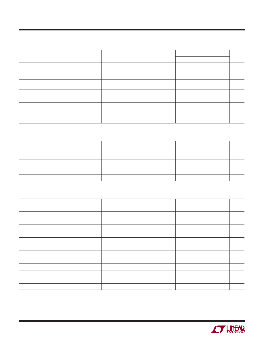
DIGITAL INPUTS AND DIGITAL OUTPUTS The l denotes the specications which apply over the
full operating temperature range, otherwise specications are at TA = 25°C. (Note 5)
POWER REQUIREMENTS
TIMING CHARACTERISTICS The l denotes the specications which apply over the full operating temperature
range, otherwise specications are at TA = 25°C. (Note 5)
The
l denotes the specications which apply over the full operating temperature
range, otherwise specications are at TA = 25°C. (Note 5)
SYMBOL
PARAMETER
CONDITIONS
LTC1863/LTC1867/LTC1867A
UNITS
MIN
TYP
MAX
VDD
Supply Voltage
(Note 9)
4.75
5.25
V
IDD
Supply Current
fSAMPLE = 200ksps
NAP Mode
SLEEP Mode
l
1.3
150
0.2
1.8
3
mA
μA
PDISS
Power Dissipation
l
6.5
9
mW
SYMBOL
PARAMETER
CONDITIONS
LTC1863/LTC1867/LTC1867A
UNITS
MIN
TYP
MAX
fSAMPLE
Maximum Sampling Frequency
l
200
kHz
tCONV
Conversion Time
l
33.5
μs
tACQ
Acquisition Time
l
1.5
1.1
μs
fSCK
SCK Frequency
40
MHz
t1
CS/CONV High Time
Short CS/CONV Pulse Mode
l
40
100
ns
t2
SDO Valid After SCK↓
CL = 25pF (Note 11)
l
13
22
ns
t3
SDO Valid Hold Time After SCK↓
CL = 25pF
l
511
ns
t4
SDO Valid After CS/CONV↓
CL = 25pF
l
10
30
ns
t5
SDI Setup Time Before SCK↑
l
15
–6
ns
t6
SDI Hold Time After SCK↑
l
10
4
ns
t7
SLEEP Mode Wake-Up Time
CREFCOMP = 10μF, CVREF = 2.2μF
60
ms
t8
Bus Relinquish Time After CS/CONV↑
CL = 25pF
l
20
40
ns
Note 1: Stresses beyond those listed under Absolute Maximum Ratings
may cause permanent damage to the device. Exposure to any Absolute
Maximum Rating condition for extended periods may affect device
reliability and lifetime
Note 2: All voltage values are with respect to GND (unless otherwise noted).
Note 3: When these pin voltages are taken below GND or above VDD, they
will be clamped by internal diodes. This product can handle input currents
of greater than 100mA without latchup.
SYMBOL
PARAMETER
CONDITIONS
LTC1863/LTC1867/LTC1867A
UNITS
MIN
TYP
MAX
CIN
Digital Input Capacitance
2pF
VOH
High Level Output Voltage (SDO)
VDD = 4.75V, IO = –10μA
VDD = 4.75V, IO = –200μA
l
4
4.75
4.74
V
VOL
Low Level Output Voltage (SDO)
VDD = 4.75V, IO = 160μA
VDD = 4.75V, IO = 1.6mA
l
0.05
0.1
0.4
V
ISOURCE
Output Source Current
SDO = 0V
–32
mA
ISINK
Output Sink Current
SDO = VDD
19
mA
Hi-Z Output Leakage
Hi-Z Output Capacitance
CS/CONV = High, SDO = 0V or VDD
CS/CONV = High (Note 10)
l
±10
15
μA
pF
Data Format
Unipolar
Bipolar
Straight Binary
Two’s Complement
相关PDF资料 |
PDF描述 |
|---|---|
| VI-2TL-IW-F3 | CONVERTER MOD DC/DC 28V 100W |
| LTC2237IUH#PBF | IC ADC 10-BIT 40MSPS 3V 32-QFN |
| AD7812YNZ | IC ADC 10BIT 8CHAN SRL 20DIP |
| VI-2TL-IW-F2 | CONVERTER MOD DC/DC 28V 100W |
| VE-J4K-MW-F4 | CONVERTER MOD DC/DC 40V 100W |
相关代理商/技术参数 |
参数描述 |
|---|---|
| LTC1863LCGN | 制造商:Linear Technology 功能描述:ADC Single SAR 175ksps 12-bit Serial 16-Pin SSOP N |
| LTC1863LCGN#PBF | 功能描述:IC ADC 12BIT 8CH 175KSPS 16SSOP RoHS:是 类别:集成电路 (IC) >> 数据采集 - 模数转换器 系列:- 标准包装:1 系列:microPOWER™ 位数:8 采样率(每秒):1M 数据接口:串行,SPI? 转换器数目:1 功率耗散(最大):- 电压电源:模拟和数字 工作温度:-40°C ~ 125°C 安装类型:表面贴装 封装/外壳:24-VFQFN 裸露焊盘 供应商设备封装:24-VQFN 裸露焊盘(4x4) 包装:Digi-Reel® 输入数目和类型:8 个单端,单极 产品目录页面:892 (CN2011-ZH PDF) 其它名称:296-25851-6 |
| LTC1863LCGN#PBF | 制造商:Linear Technology 功能描述:ADC, 8CH, 12BIT, 175KSPS, SSOP-16 |
| LTC1863LCGN#TR | 制造商:Linear Technology 功能描述:ADC Single SAR 175ksps 12-bit Serial 16-Pin SSOP N T/R |
| LTC1863LCGN#TRPBF | 功能描述:IC ADC 12BIT 8CH 175KSPS 16SSOP RoHS:是 类别:集成电路 (IC) >> 数据采集 - 模数转换器 系列:- 标准包装:1,000 系列:- 位数:16 采样率(每秒):45k 数据接口:串行 转换器数目:2 功率耗散(最大):315mW 电压电源:模拟和数字 工作温度:0°C ~ 70°C 安装类型:表面贴装 封装/外壳:28-SOIC(0.295",7.50mm 宽) 供应商设备封装:28-SOIC W 包装:带卷 (TR) 输入数目和类型:2 个单端,单极 |
发布紧急采购,3分钟左右您将得到回复。