- 您现在的位置:买卖IC网 > PDF目录10667 > LTC1867LACGN#PBF (Linear Technology)IC ADC 16BIT 8CH 175KSPS 16SSOP PDF资料下载
参数资料
| 型号: | LTC1867LACGN#PBF |
| 厂商: | Linear Technology |
| 文件页数: | 5/16页 |
| 文件大小: | 0K |
| 描述: | IC ADC 16BIT 8CH 175KSPS 16SSOP |
| 标准包装: | 100 |
| 位数: | 16 |
| 采样率(每秒): | 175k |
| 数据接口: | MICROWIRE?,串行,SPI? |
| 转换器数目: | 1 |
| 功率耗散(最大): | 2.7mW |
| 电压电源: | 单电源 |
| 工作温度: | 0°C ~ 70°C |
| 安装类型: | 表面贴装 |
| 封装/外壳: | 16-SSOP(0.154",3.90mm 宽) |
| 供应商设备封装: | 16-SSOP |
| 包装: | 管件 |
| 输入数目和类型: | 8 个单端,单极;8 个单端,双极;4 个差分,单极;4 个差分,双极 |
| 产品目录页面: | 1347 (CN2011-ZH PDF) |
| 配用: | DC873A-ND - BOARD SAR ADC LTC1867L DC806A-ND - BOARD SAR ADC LTC1867 |
LTC1863L/LTC1867L
13
1863l7lfc
APPLICATIONS INFORMATION
If the CS/CONV returns low during a bit decision, it can
create a small error. For best performance ensure that the
CS/CONV returns low either within 100ns after the conver-
sion starts (i.e. before the rst bit decision) or after the
conversion ends. If CS/CONV is low when the conversion
ends, the MSB bit will appear on SDO at the end of the
conversion and the ADC will remain powered up.
Sleep Mode
If the SLP = 1 is selected in the input word, the ADC will
enter SLEEP mode and draw only leakage current (pro-
vided that all the digital inputs stay at GND or VDD). After
release from the SLEEP mode, the ADC needs 80ms to
wake up (charge the 2.2μF/10μF bypass capacitors on
VREF/REFCOMP pins).
Board Layout and Bypassing
To obtain the best performance, a printed circuit board
with a ground plane is required. Layout for the printed
circuit board should ensure digital and analog signal lines
are separated as much as possible. In particular, care
should be taken not to run any digital signal alongside
an analog signal.
All analog inputs should be screened by GND. VREF, REF-
COMP and VDD should be bypassed to this ground plane
as close to the pin as possible; the low impedance of the
common return for these bypass capacitors is essential
to the low noise operation of the ADC. The width for these
tracks should be as wide as possible.
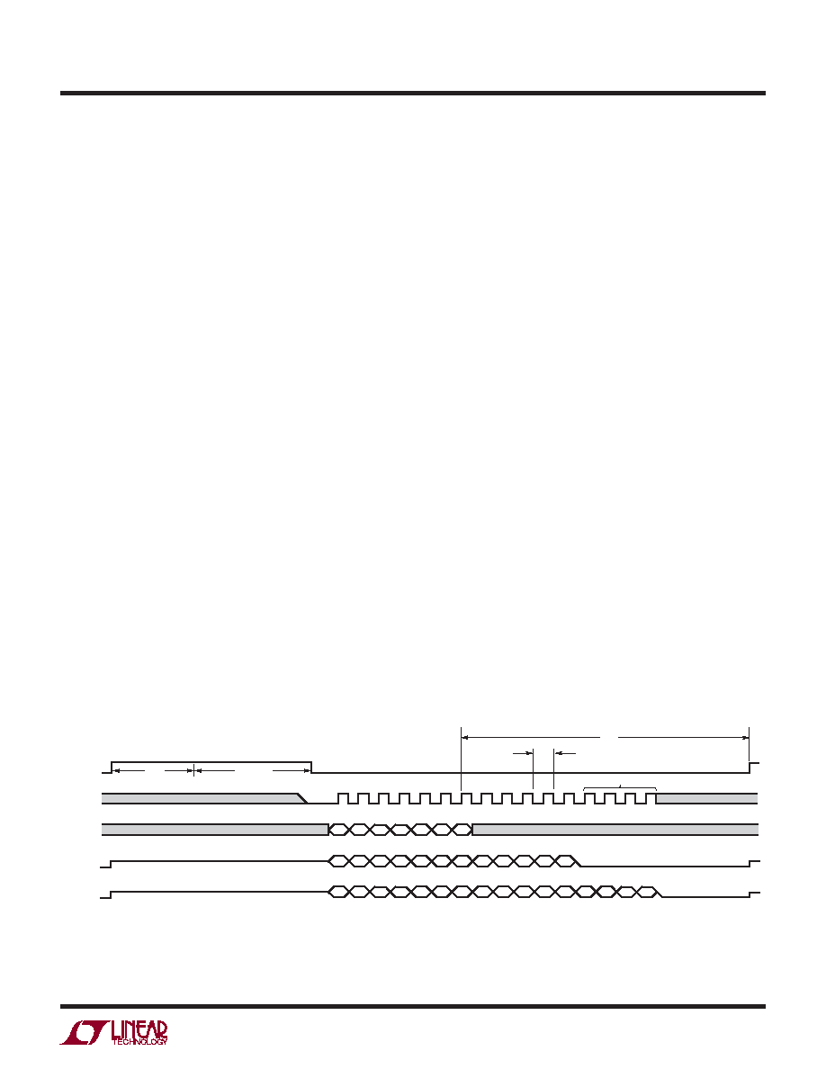
Timing and Control
Conversion start is controlled by the CS/CONV digital in-
put. The rising edge transition of the CS/CONV will start a
conversion. Once initiated, it cannot be restarted until the
conversion is complete. Figures 6 and 7 show the timing
diagrams for two types of CS/CONV pulses.
Example 1 (Figure 6) shows the LTC1863L/LTC1867L
operating in automatic nap mode with CS/CONV signal
staying HIGH after the conversion. Automatic nap mode
provides power reduction at reduced sample rate.
The ADCs can also operate with the CS/CONV signal
returning LOW before the conversion ends. In this mode
(Example 2, Figure 7), the ADCs remain powered up. The
digital output, SDO, will go HIGH immediately after the
conversion is complete if the analog inputs are above
half scale in unipolar mode or below half scale in bipolar
mode. This is a way to measure the conversion time of
the A/D converter.
For best performance, it is recommended to keep SCK, SDI,
and SDO at a constant logic high or low during acquisition
and conversion, even though these signals may be ignored
by the serial interface (DON’T CARE). Communication
with other devices on the bus should not coincide with
the conversion period (tCONV).
Figures 8 and 9 are the transfer characteristics for the
bipolar and unipolar mode.
S0
SD
0S
S1
COM UNI
SLP
D11
D10
D9
D8
D7
D6
D5
D4
D3
D2
D1
D0
1/fSCK
tACQ
CS/CONV
SCK
SDI
SDO
(LTC1863)
Hi-Z
D12
D15
D14
D13
D11
D10
D9
D8
D7
D6
D5
D4
D3
D2
D1
D0
Hi-Z
123456789
10
11
12
13
14
15
16
1863L7L F06
DON'T CARE
NOT NEEDED FOR LTC1863
tCONV
NAP MODE
SDO
(LTC1867)
MSB
DON'T CARE
Figure 6. Example 1, CS/CONV Starts a Conversion and Remains HIGH Until Next Data Transfer. With CS/CONV
Remaining HIGH After the Conversion, Automatic Nap Modes Provides Power Reduction at Reduced Sample Rate
相关PDF资料 |
PDF描述 |
|---|---|
| VE-JT2-MY-F3 | CONVERTER MOD DC/DC 15V 50W |
| VE-212-MX | CONVERTER MOD DC/DC 15V 75W |
| MAX3051EKA+T | IC TXRX CAN 3.3V SOT23-8 |
| VE-JT2-MY-F2 | CONVERTER MOD DC/DC 15V 50W |
| VI-B12-MX-F4 | CONVERTER MOD DC/DC 15V 75W |
相关代理商/技术参数 |
参数描述 |
|---|---|
| LTC1867LAIGN | 制造商:Linear Technology 功能描述:MS-ADC/General Purpose, 16-bit, 8-ch. Serial, Micropower ADC |
| LTC1867LAIGN#PBF | 功能描述:IC ADC 16BIT 8CH 175KSPS 16SSOP RoHS:是 类别:集成电路 (IC) >> 数据采集 - 模数转换器 系列:- 标准包装:1 系列:microPOWER™ 位数:8 采样率(每秒):1M 数据接口:串行,SPI? 转换器数目:1 功率耗散(最大):- 电压电源:模拟和数字 工作温度:-40°C ~ 125°C 安装类型:表面贴装 封装/外壳:24-VFQFN 裸露焊盘 供应商设备封装:24-VQFN 裸露焊盘(4x4) 包装:Digi-Reel® 输入数目和类型:8 个单端,单极 产品目录页面:892 (CN2011-ZH PDF) 其它名称:296-25851-6 |
| LTC1867LAIGN#TRPBF | 功能描述:IC ADC 16BIT 8CH 175KSPS 16SSOP RoHS:是 类别:集成电路 (IC) >> 数据采集 - 模数转换器 系列:- 标准包装:1,000 系列:- 位数:12 采样率(每秒):300k 数据接口:并联 转换器数目:1 功率耗散(最大):75mW 电压电源:单电源 工作温度:0°C ~ 70°C 安装类型:表面贴装 封装/外壳:24-SOIC(0.295",7.50mm 宽) 供应商设备封装:24-SOIC 包装:带卷 (TR) 输入数目和类型:1 个单端,单极;1 个单端,双极 |
| LTC1867LCGN | 制造商:Linear Technology 功能描述:ADC Single SAR 175ksps 16-bit Serial 16-Pin SSOP N |
| LTC1867LCGN#PBF | 功能描述:IC ADC 16BIT 8CH 175KSPS 16SSOP RoHS:是 类别:集成电路 (IC) >> 数据采集 - 模数转换器 系列:- 标准包装:1,000 系列:- 位数:12 采样率(每秒):300k 数据接口:并联 转换器数目:1 功率耗散(最大):75mW 电压电源:单电源 工作温度:0°C ~ 70°C 安装类型:表面贴装 封装/外壳:24-SOIC(0.295",7.50mm 宽) 供应商设备封装:24-SOIC 包装:带卷 (TR) 输入数目和类型:1 个单端,单极;1 个单端,双极 |
发布紧急采购,3分钟左右您将得到回复。