- 您现在的位置:买卖IC网 > PDF目录296328 > LTC1867TA1P2 Optoelectronic PDF资料下载
参数资料
| 型号: | LTC1867TA1P2 |
| 英文描述: | Optoelectronic |
| 中文描述: | 光电 |
| 文件页数: | 20/20页 |
| 文件大小: | 278K |
| 代理商: | LTC1867TA1P2 |
9
LTC1864/LTC1865
18645f
LTC1864 OPERATION
Operating Sequence
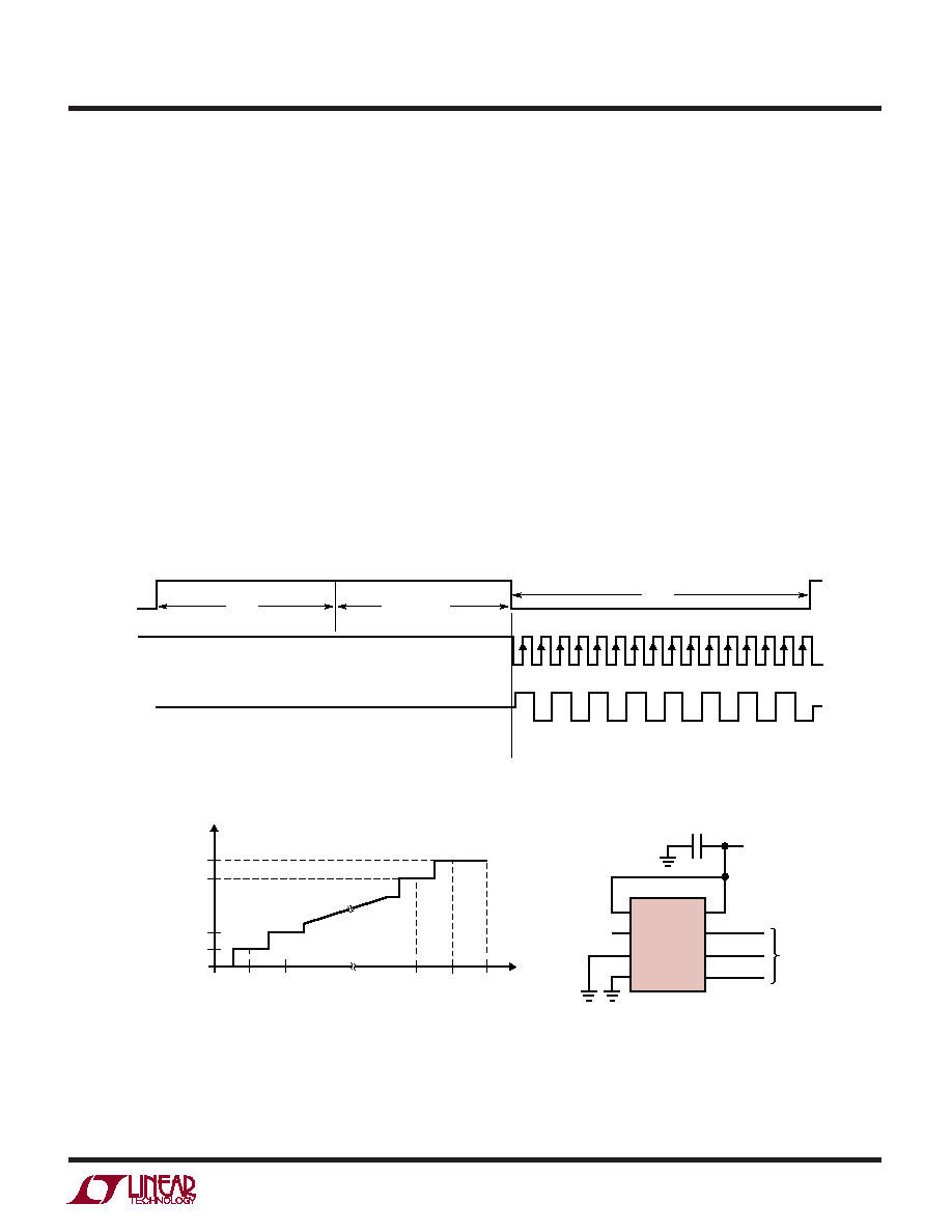
The LTC1864 conversion cycle begins with the rising edge
of CONV. After a period equal to tCONV, the conversion is
finished. If CONV is left high after this time, the LTC1864
goes into sleep mode drawing only leakage current. On the
falling edge of CONV, the LTC1864 goes into sample mode
and SDO is enabled. SCK synchronizes the data transfer
with each bit being transmitted from SDO on the falling
SCK edge. The receiving system should capture the data
from SDO on the rising edge of SCK. After completing the
data transfer, if further SCK clocks are applied with CONV
low, SDO will output zeros indefinitely. See Figure 1.
Analog Inputs
The LTC1864 has a unipolar differential analog input. The
converter will measure the voltage between the “IN+” and
“IN–” inputs. A zero code will occur when IN+ minus IN–
equals zero. Full scale occurs when IN+ minus IN– equals
VREF minus 1LSB. See Figure 2. Both the “IN+” and
“IN–” inputs are sampled at the same time, so common
mode noise on the inputs is rejected by the ADC. If “IN–”
is grounded and VREF is tied to VCC, a rail-to-rail input span
will result on “IN+” as shown in Figure 3.
Reference Input
The voltage on the reference input of the LTC1864 defines
the full-scale range of the A/D converter. The LTC1864 can
operate with reference voltages from VCC to 1V.
CONV
tCONV
SCK
SDO
16
15
14
13
12
11
10
9
8
7
6
5
4
3
2
1
B15 B14
B12
B10
B8
B6
B4
B2
B0*
Hi-Z
1854 F01
Hi-Z
B13
B11
B9
B7
B5
B3
B1
SLEEP MODE
tSMPL
*AFTER COMPLETING THE DATA TRANSFER, IF FURTHER SCK CLOCKS ARE
APPLIED WITH CONV LOW, THE ADC WILL OUTPUT ZEROS INDEFINITELY
1
2
3
4
8
7
6
5
VREF
IN+
IN–
GND
VCC
SCK
SDO
CONV
LTC1864
1864 F03
VIN = 0V TO VCC
VCC
1
F
SERIAL DATA LINK TO
ASIC, PLD, MPU, DSP
OR SHIFT REGISTERS
Figure 1. LTC1864 Operating Sequence
Figure 3. LTC1864 with Rail-to-Rail Input Span
Figure 2. LTC1864 Transfer Curve
0V
1LSB
V
REF
–
2LSB
V
REF
–
1LSB
V
REF
VIN*
*VIN = IN
+ – IN–
0 0 0 0 0 0 0 0 0 0 0 0 0 0 0 1
0 0 0 0 0 0 0 0 0 0 0 0 0 0 0 0
1 1 1 1 1 1 1 1 1 1 1 1 1 1 1 1
1 1 1 1 1 1 1 1 1 1 1 1 1 1 1 0
1864 F02
APPLICATIO S I FOR ATIO
WU
UU
相关PDF资料 |
PDF描述 |
|---|---|
| LTC2050HVCS8 | Chopper-Stabilized Operational Amplifier |
| LTC2050HVIS5 | Chopper-Stabilized Operational Amplifier |
| LTC2050HVIS6 | Chopper-Stabilized Operational Amplifier |
| LTC2050HVIS8 | Chopper-Stabilized Operational Amplifier |
| LTC2051CMS10 | OP-AMP|DUAL|CMOS|TSSOP|10PIN|PLASTIC |
相关代理商/技术参数 |
参数描述 |
|---|---|
| LTC1871EMS | 功能描述:IC REG CTRLR BST FLYBK CM 10MSOP RoHS:否 类别:集成电路 (IC) >> PMIC - 稳压器 - DC DC 切换控制器 系列:- 标准包装:2,500 系列:- PWM 型:电流模式 输出数:1 频率 - 最大:500kHz 占空比:96% 电源电压:4 V ~ 36 V 降压:无 升压:是 回扫:无 反相:无 倍增器:无 除法器:无 Cuk:无 隔离:无 工作温度:-40°C ~ 125°C 封装/外壳:24-WQFN 裸露焊盘 包装:带卷 (TR) |
| LTC1871EMS#PBF | 功能描述:IC REG CTRLR BST FLYBK CM 10MSOP RoHS:是 类别:集成电路 (IC) >> PMIC - 稳压器 - DC DC 切换控制器 系列:- 特色产品:LM3753/54 Scalable 2-Phase Synchronous Buck Controllers 标准包装:1 系列:PowerWise® PWM 型:电压模式 输出数:1 频率 - 最大:1MHz 占空比:81% 电源电压:4.5 V ~ 18 V 降压:是 升压:无 回扫:无 反相:无 倍增器:无 除法器:无 Cuk:无 隔离:无 工作温度:-5°C ~ 125°C 封装/外壳:32-WFQFN 裸露焊盘 包装:Digi-Reel® 产品目录页面:1303 (CN2011-ZH PDF) 其它名称:LM3754SQDKR |
| LTC1871EMS#TR | 功能描述:IC REG CTRLR BST FLYBK CM 10MSOP RoHS:否 类别:集成电路 (IC) >> PMIC - 稳压器 - DC DC 切换控制器 系列:- 标准包装:2,500 系列:- PWM 型:电流模式 输出数:1 频率 - 最大:500kHz 占空比:96% 电源电压:4 V ~ 36 V 降压:无 升压:是 回扫:无 反相:无 倍增器:无 除法器:无 Cuk:无 隔离:无 工作温度:-40°C ~ 125°C 封装/外壳:24-WQFN 裸露焊盘 包装:带卷 (TR) |
| LTC1871EMS#TRPBF | 功能描述:IC REG CTRLR BST FLYBK CM 10MSOP RoHS:是 类别:集成电路 (IC) >> PMIC - 稳压器 - DC DC 切换控制器 系列:- 标准包装:2,500 系列:- PWM 型:电流模式 输出数:1 频率 - 最大:500kHz 占空比:96% 电源电压:4 V ~ 36 V 降压:无 升压:是 回扫:无 反相:无 倍增器:无 除法器:无 Cuk:无 隔离:无 工作温度:-40°C ~ 125°C 封装/外壳:24-WQFN 裸露焊盘 包装:带卷 (TR) |
| LTC1871EMS-1#PBF | 功能描述:IC REG CTRLR BST FLYBK CM 10MSOP RoHS:是 类别:集成电路 (IC) >> PMIC - 稳压器 - DC DC 切换控制器 系列:- 标准包装:2,500 系列:- PWM 型:电流模式 输出数:1 频率 - 最大:500kHz 占空比:96% 电源电压:4 V ~ 36 V 降压:无 升压:是 回扫:无 反相:无 倍增器:无 除法器:无 Cuk:无 隔离:无 工作温度:-40°C ~ 125°C 封装/外壳:24-WQFN 裸露焊盘 包装:带卷 (TR) |
发布紧急采购,3分钟左右您将得到回复。