- 您现在的位置:买卖IC网 > PDF目录15265 > LTC1873EG#TRPBF (Linear Technology)IC REG CTRLR BUCK PWM VM 28-SSOP PDF资料下载
参数资料
| 型号: | LTC1873EG#TRPBF |
| 厂商: | Linear Technology |
| 文件页数: | 11/32页 |
| 文件大小: | 0K |
| 描述: | IC REG CTRLR BUCK PWM VM 28-SSOP |
| 标准包装: | 2,000 |
| PWM 型: | 电压模式 |
| 输出数: | 2 |
| 频率 - 最大: | 750kHz |
| 占空比: | 93% |
| 电源电压: | 3 V ~ 7 V |
| 降压: | 是 |
| 升压: | 无 |
| 回扫: | 无 |
| 反相: | 无 |
| 倍增器: | 无 |
| 除法器: | 无 |
| Cuk: | 无 |
| 隔离: | 无 |
| 工作温度: | -40°C ~ 85°C |
| 封装/外壳: | 28-SSOP(0.209",5.30mm 宽) |
| 包装: | 带卷 (TR) |
第1页第2页第3页第4页第5页第6页第7页第8页第9页第10页当前第11页第12页第13页第14页第15页第16页第17页第18页第19页第20页第21页第22页第23页第24页第25页第26页第27页第28页第29页第30页第31页第32页
�� �
�
�LTC1873�
�APPLICATIO� S� I� FOR� ATIO�
�pin.� The� output� is� connected� to� COMP,� which� is� in� turn�
�connected� to� the� soft-start� circuitry� and� from� there� to� the�
�PWM� generator.�
�Unlike� many� regulators� that� use� a� resistor� divider� con-�
�nected� to� a� high� impedance� feedback� input,� the� LTC1873�
�is� designed� to� use� an� inverting� summing� amplifier� topol-�
�ogy� with� the� FB� pin� configured� as� a� virtual� ground.� This�
�allows� flexibility� in� choosing� pole� and� zero� locations� not�
�available� with� simple� g� m� configurations.� In� particular,� it�
�allows� the� use� of� “type� 3”� compensation,� which� provides�
�a� phase� boost� at� the� LC� pole� frequency� and� significantly�
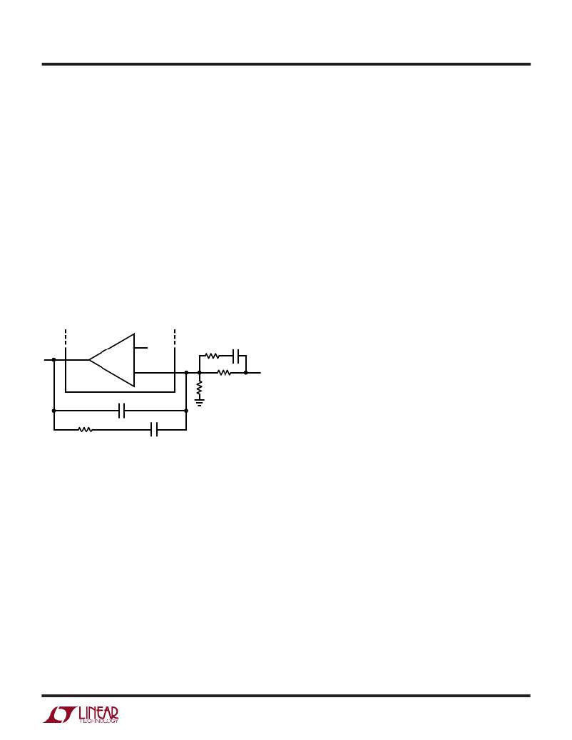
�improves� loop� phase� margin� (see� Figure� 3).� The� Feedback�
�Loop/Compensation� section� contains� a� detailed� explana-�
�tion� of� type� 3� feedback� loops.� Note� that� side� 1� of� the�
�LTC1873� includes� R1� and� R� B� internally� as� part� of� the� VID�
�DAC� circuitry.�
�to� resume� normal� operation� when� the� fault� is� removed.�
�The� overvoltage� protection� circuit� can� optionally� be� set� to�
�latch� the� output� off� permanently� (see� the� Overvoltage� Fault�
�section).�
�The� MIN� comparator� (see� Block� Diagram)� trips� whenever�
�FB� is� more� than� 5%� below� 800mV� and� immediately� forces�
�the� switch� duty� cycle� to� 90%� to� bring� the� output� voltage�
�back� into� range.� It� releases� when� FB� is� within� the� 5%�
�window.� MIN� is� disabled� when� the� soft-start� or� current�
�limit� circuits� are� active� —the� only� two� times� that� the�
�output� should� legitimately� be� below� its� regulated� value.�
�Notice� that� the� FB� pin� is� the� virtual� ground� node� of� the�
�feedback� amplifier.� A� typical� compensation� network� does�
�not� include� local� DC� feedback� around� the� amplifier,� so� that�
�the� DC� level� at� FB� will� be� an� accurate� replica� of� the� output�
�voltage,� divided� down� by� R1� and� R� B� (Figure� 3).� However,�
�the� compensation� capacitors� will� tend� to� attenuate� AC�
�COMP�
�FB�
�+�
�–�
�0.8V�
�FB�
�R3�
�R1�
�C3�
�V� OUT�
�signals� at� FB,� especially� with� low� bandwidth� type� 1� feed-�
�back� loops.� This� creates� a� situation� where� the� MIN� and�
�MAX� comparators� do� not� respond� immediately� to� shifts� in�
�the� output� voltage,� since� they� monitor� the� output� at� FB.�
�R2�
�C2�
�C1�
�R� B�
�1873� F03�
�Maximizing� feedback� loop� bandwidth� will� minimize� these�
�delays� and� allow� MIN� and� MAX� to� operate� properly.� See�
�the� Feedback� Loop/Compensation� section.�
�Figure� 3.� “Type� 3”� Feedback� Loop� (Side� 2� Shown)�
�MIN/MAX� COMPARATORS�
�Two� additional� feedback� loops� keep� an� eye� on� the� primary�
�feedback� amplifier� and� step� in� if� the� feedback� node� moves�
�±� 5%� from� its� nominal� 800mV� value.� The� MAX� comparator�
�(see� Block� Diagram)� activates� whenever� FB� rises� more�
�than� 5%� above� 800mV.� It� immediately� turns� the� top�
�MOSFET� (QT)� off� and� the� bottom� MOSFET� (QB)� on� and�
�keeps� them� that� way� until� FB� falls� back� within� 5%� of� its�
�nominal� value.� This� pulls� the� output� down� as� fast� as�
�possible,� preventing� damage� to� the� (often� expensive)�
�load.� If� FB� rises� because� the� output� is� shorted� to� a� higher�
�supply,� QB� will� stay� on� until� the� short� goes� away,� the�
�higher� supply� current� limits� or� QB� dies� trying� to� save� the�
�load.� This� behavior� provides� maximum� protection� against�
�SHUTDOWN/SOFT-START�
�Each� half� of� the� LTC1873� has� a� RUN/SS� pin.� The� RUN/SS�
�pins� perform� two� functions:� when� pulled� to� ground,� each�
�shuts� down� its� half� of� the� LTC1873,� and� each� acts� as� a�
�conventional� soft-start� pin,� enforcing� a� maximum� duty�
�cycle� limit� proportional� to� the� voltage� at� RUN/SS.� An�
�internal� 3.5� μ� A� current� source� pull-up� is� connected� to� each�
�RUN/SS� pin,� allowing� a� soft-start� ramp� to� be� generated�
�with� a� single� external� capacitor� to� ground.� The� 3.5� μ� A�
�current� sources� are� active� even� when� the� LTC1873� is� shut�
�down,� ensuring� the� device� will� start� when� any� external�
�pull-down� at� RUN/SS� is� released.� Either� side� can� be� shut�
�down� without� affecting� the� operation� of� the� other� side.� If�
�both� sides� are� shut� down� at� the� same� time,� the� LTC1873�
�goes� into� a� micropower� sleep� mode,� and� quiescent� cur-�
�rent� drops� typically� below� 50� μ� A.� Entering� sleep� mode� also�
�resets� the� FAULT� latch,� if� it� was� set.�
�overvoltage� faults� at� the� output,� while� allowing� the� circuit�
�11�
�相关PDF资料 |
PDF描述 |
|---|---|
| H2AXT-10112-W4-ND | JUMPER-H1502TR/A2015W/X 12" |
| LTC1159CG-5 | IC REG CTRLR BUCK PWM CM 20-SSOP |
| LTC1159CG-3.3#PBF | IC REG CTRLR BUCK PWM CM 20-SSOP |
| LTC1159CG-3.3 | IC REG CTRLR BUCK PWM CM 20-SSOP |
| H2AXT-10112-V4-ND | JUMPER-H1502TR/A2015V/X 12" |
相关代理商/技术参数 |
参数描述 |
|---|---|
| LTC1874EGN | 功能描述:IC REG CTRLR BUCK PWM CM 16-SSOP RoHS:否 类别:集成电路 (IC) >> PMIC - 稳压器 - DC DC 切换控制器 系列:- 标准包装:2,500 系列:- PWM 型:电流模式 输出数:1 频率 - 最大:500kHz 占空比:96% 电源电压:4 V ~ 36 V 降压:无 升压:是 回扫:无 反相:无 倍增器:无 除法器:无 Cuk:无 隔离:无 工作温度:-40°C ~ 125°C 封装/外壳:24-WQFN 裸露焊盘 包装:带卷 (TR) |
| LTC1874EGN#PBF | 功能描述:IC REG CTRLR BUCK PWM CM 16-SSOP RoHS:是 类别:集成电路 (IC) >> PMIC - 稳压器 - DC DC 切换控制器 系列:- 标准包装:2,500 系列:- PWM 型:电流模式 输出数:1 频率 - 最大:500kHz 占空比:96% 电源电压:4 V ~ 36 V 降压:无 升压:是 回扫:无 反相:无 倍增器:无 除法器:无 Cuk:无 隔离:无 工作温度:-40°C ~ 125°C 封装/外壳:24-WQFN 裸露焊盘 包装:带卷 (TR) |
| LTC1874EGN#TR | 功能描述:IC REG CTRLR BUCK PWM CM 16-SSOP RoHS:否 类别:集成电路 (IC) >> PMIC - 稳压器 - DC DC 切换控制器 系列:- 标准包装:2,500 系列:- PWM 型:电流模式 输出数:1 频率 - 最大:500kHz 占空比:96% 电源电压:4 V ~ 36 V 降压:无 升压:是 回扫:无 反相:无 倍增器:无 除法器:无 Cuk:无 隔离:无 工作温度:-40°C ~ 125°C 封装/外壳:24-WQFN 裸露焊盘 包装:带卷 (TR) |
| LTC1874EGN#TRPBF | 功能描述:IC REG CTRLR BUCK PWM CM 16-SSOP RoHS:是 类别:集成电路 (IC) >> PMIC - 稳压器 - DC DC 切换控制器 系列:- 标准包装:2,500 系列:- PWM 型:电流模式 输出数:1 频率 - 最大:500kHz 占空比:96% 电源电压:4 V ~ 36 V 降压:无 升压:是 回扫:无 反相:无 倍增器:无 除法器:无 Cuk:无 隔离:无 工作温度:-40°C ~ 125°C 封装/外壳:24-WQFN 裸露焊盘 包装:带卷 (TR) |
| LTC1875EGN | 功能描述:IC REG BUCK SYNC ADJ 1.5A 16SSOP RoHS:否 类别:集成电路 (IC) >> PMIC - 稳压器 - DC DC 开关稳压器 系列:- 标准包装:2,500 系列:- 类型:降压(降压) 输出类型:固定 输出数:1 输出电压:1.2V,1.5V,1.8V,2.5V 输入电压:2.7 V ~ 20 V PWM 型:- 频率 - 开关:- 电流 - 输出:50mA 同步整流器:是 工作温度:-40°C ~ 125°C 安装类型:表面贴装 封装/外壳:10-TFSOP,10-MSOP(0.118",3.00mm 宽)裸露焊盘 包装:带卷 (TR) 供应商设备封装:10-MSOP 裸露焊盘 |
发布紧急采购,3分钟左右您将得到回复。