- 您现在的位置:买卖IC网 > PDF目录44988 > LTC1877IMS8#TRPBF (LINEAR TECHNOLOGY CORP) 1.5 A SWITCHING REGULATOR, 605 kHz SWITCHING FREQ-MAX, PDSO8 PDF资料下载
参数资料
| 型号: | LTC1877IMS8#TRPBF |
| 厂商: | LINEAR TECHNOLOGY CORP |
| 元件分类: | 稳压器 |
| 英文描述: | 1.5 A SWITCHING REGULATOR, 605 kHz SWITCHING FREQ-MAX, PDSO8 |
| 封装: | LEAD FREE, PLASTIC, MSOP-8 |
| 文件页数: | 3/16页 |
| 文件大小: | 234K |
| 代理商: | LTC1877IMS8#TRPBF |
LTC1877
11
1877fa
this stable operating point the phase comparator output
is high impedance and the lter capacitor CLP holds the
voltage.
The loop lter components CLP and RLP smooth out the
current pulses from the phase detector and provide a
stable input to the voltage controlled oscillator. The lter
component’s CLP and RLP determine how fast the loop
acquires lock. Typically RLP = 10k and CLP is 2200pF
to 0.01μF. When not synchronized to an external clock,
the internal connection to the VCO is disconnected. This
disallows setting the internal oscillator frequency by a DC
voltage on the VPLL LPF pin.
Efciency Considerations
The efciency of a switching regulator is equal to the output
power divided by the input power times 100%. It is often
useful to analyze individual losses to determine what is
limiting the efciency and which change would produce
the most improvement. Efciency can be expressed as:
Efciency = 100% – (L1 + L2 + L3 + ...)
where L1, L2, etc. are the individual losses as a percent-
age of input power.
Although all dissipative elements in the circuit produce
losses, two main sources usually account for most of
the losses in LTC1877 circuits: VIN quiescent current and
I2R losses. The VIN quiescent current loss dominates the
efciency loss at very low load currents, whereas the
I2R loss dominates the efciency loss at medium to high
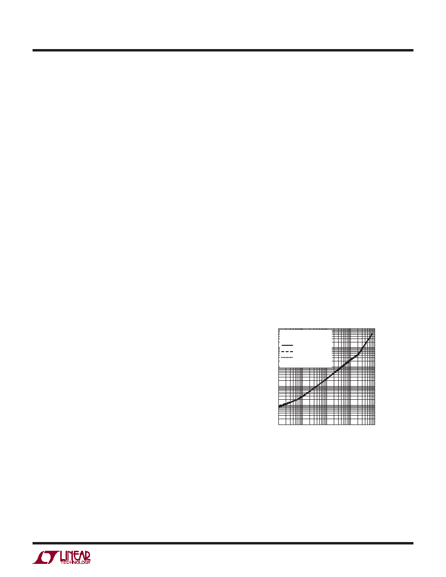
load currents. In a typical efciency plot, the efciency
curve at very low load currents can be misleading since
the actual power lost is of no consequence, as illustrated
in Figure 6.
1. The VIN quiescent current is due to two components:
the DC bias current as given in the Electrical Charac-
teristics section and the internal main switch and syn-
chronous switch gate charge currents. The gate charge
current results from switching the gate capacitance
of the internal power MOSFET switches. Each time
the gate is switched from high to low to high again, a
packet of charge dQ moves from VIN to ground. The
resulting dQ/dt is the current out of VIN that is typically
larger than the DC bias current. In continuous mode,
IGATECHG = f(QT + QB) where QT and QB are the gate
charges of the internal top and bottom switches. Both
the DC bias and gate charge losses are proportional
to VIN and thus their effects will be more pronounced
at higher supply voltages.
2. I2R losses are calculated from the resistances of the
internal switches, RSW, and external inductor RL. In
continuous mode, the average output current ow-
ing through inductor L is chopped between the main
switch and the synchronous switch. Thus, the series
resistance looking into the SW pin is a function of both
top and bottom MOSFET RDS(ON) and the duty cycle
(DC) as follows:
RSW = (RDS(ON)TOP)(DC) + (RDS(ON)BOT)(1 – DC)
The RDS(ON) for both the top and bottom MOSFETs can
be obtained from the Typical Performance Character-
istics curves. Thus, to obtain I2R losses, simply add
RSW to RL and multiply the result by the square of the
average output current.
Other losses including CIN and COUT ESR dissipative los-
ses and inductor core losses generally account for less
than 2% total additional loss.
LOAD CURRENT (mA)
0.1
1
0.00001
POWER
LOST
(W)
0.001
1
10
100
1000
1877 F06
0.0001
0.01
0.1
VOUT = 1.5V
VOUT = 2.5V
VOUT = 3.3V
VIN = 4.2V
L = 10μH
Burst Mode OPERATION
Figure 6. Power Lost vs Load Current
Thermal Considerations
In most applications the LTC1877 does not dissipate much
heat due to its high efciency. But, in applications where the
LTC1877 is running at high ambient temperature with low
supply voltage and high duty cycles, such as in dropout,
the heat dissipated may exceed the maximum junction
APPLICATIONS INFORMATION
相关PDF资料 |
PDF描述 |
|---|---|
| LTC1929IG-PG | 3 A DUAL SWITCHING CONTROLLER, 310 kHz SWITCHING FREQ-MAX, PDSO28 |
| LTC203MJ/883B | QUAD 1-CHANNEL, SGL POLE SGL THROW SWITCH, CDIP16 |
| LTC202MJ/883B | QUAD 1-CHANNEL, SGL POLE SGL THROW SWITCH, CDIP16 |
| LTC201AMJ/883B | QUAD 1-CHANNEL, SGL POLE SGL THROW SWITCH, CDIP16 |
| LTC2904IDDB8 | 2-CHANNEL POWER SUPPLY SUPPORT CKT, PDSO8 |
相关代理商/技术参数 |
参数描述 |
|---|---|
| LTC1878EMS8 | 功能描述:IC REG BUCK SYNC ADJ 0.6A 8MSOP RoHS:否 类别:集成电路 (IC) >> PMIC - 稳压器 - DC DC 开关稳压器 系列:- 标准包装:2,500 系列:- 类型:升压(升压) 输出类型:可调式 输出数:1 输出电压:1.24 V ~ 30 V 输入电压:1.5 V ~ 12 V PWM 型:电流模式,混合 频率 - 开关:600kHz 电流 - 输出:500mA 同步整流器:无 工作温度:-40°C ~ 85°C 安装类型:表面贴装 封装/外壳:8-SOIC(0.154",3.90mm 宽) 包装:带卷 (TR) 供应商设备封装:8-SOIC |
| LTC1878EMS8#PBF | 功能描述:IC REG BUCK SYNC ADJ 0.6A 8MSOP RoHS:是 类别:集成电路 (IC) >> PMIC - 稳压器 - DC DC 开关稳压器 系列:- 标准包装:250 系列:- 类型:降压(降压) 输出类型:固定 输出数:1 输出电压:1.2V 输入电压:2.05 V ~ 6 V PWM 型:电压模式 频率 - 开关:2MHz 电流 - 输出:500mA 同步整流器:是 工作温度:-40°C ~ 85°C 安装类型:表面贴装 封装/外壳:6-UFDFN 包装:带卷 (TR) 供应商设备封装:6-SON(1.45x1) 产品目录页面:1032 (CN2011-ZH PDF) 其它名称:296-25628-2 |
| LTC1878EMS8#TR | 功能描述:IC REG BUCK SYNC ADJ 0.6A 8MSOP RoHS:否 类别:集成电路 (IC) >> PMIC - 稳压器 - DC DC 开关稳压器 系列:- 标准包装:2,500 系列:- 类型:升压(升压) 输出类型:可调式 输出数:1 输出电压:1.24 V ~ 30 V 输入电压:1.5 V ~ 12 V PWM 型:电流模式,混合 频率 - 开关:600kHz 电流 - 输出:500mA 同步整流器:无 工作温度:-40°C ~ 85°C 安装类型:表面贴装 封装/外壳:8-SOIC(0.154",3.90mm 宽) 包装:带卷 (TR) 供应商设备封装:8-SOIC |
| LTC1878EMS8#TRPBF | 功能描述:IC REG BUCK SYNC ADJ 0.6A 8MSOP RoHS:是 类别:集成电路 (IC) >> PMIC - 稳压器 - DC DC 开关稳压器 系列:- 标准包装:2,500 系列:- 类型:升压(升压) 输出类型:可调式 输出数:1 输出电压:1.24 V ~ 30 V 输入电压:1.5 V ~ 12 V PWM 型:电流模式,混合 频率 - 开关:600kHz 电流 - 输出:500mA 同步整流器:无 工作温度:-40°C ~ 85°C 安装类型:表面贴装 封装/外壳:8-SOIC(0.154",3.90mm 宽) 包装:带卷 (TR) 供应商设备封装:8-SOIC |
| LTC1878EMS8PBF | 制造商:Linear Technology 功能描述: 制造商:Linear Technology 功能描述:DC-DC Converter Step-Down 2.65-6V MSOP8 |
发布紧急采购,3分钟左右您将得到回复。