- 您现在的位置:买卖IC网 > PDF目录15117 > LTC1922EN-1#PBF (Linear Technology)IC REG CTRLR ISO PWM CM/VM 20DIP PDF资料下载
参数资料
| 型号: | LTC1922EN-1#PBF |
| 厂商: | Linear Technology |
| 文件页数: | 21/24页 |
| 文件大小: | 0K |
| 描述: | IC REG CTRLR ISO PWM CM/VM 20DIP |
| 标准包装: | 18 |
| PWM 型: | 电流/电压模式 |
| 输出数: | 1 |
| 频率 - 最大: | 1MHz |
| 占空比: | 99% |
| 电源电压: | 3.8 V ~ 10.3 V |
| 降压: | 无 |
| 升压: | 无 |
| 回扫: | 无 |
| 反相: | 无 |
| 倍增器: | 无 |
| 除法器: | 无 |
| Cuk: | 无 |
| 隔离: | 是 |
| 工作温度: | -40°C ~ 85°C |
| 封装/外壳: | 20-DIP(0.300",7.62mm) |
| 包装: | 管件 |
�� �
�
�LTC1922-1�
�OPERATIO�
�slower.� A� linearized� SPICE� macromodel� of� the� control� loop�
�is� very� helpful� tool� to� quickly� evaluate� the� frequency�
�response� of� various� compensation� networks.�
�Polymer� Electrolytic� (see� Figure� 12)� 1/(2� π� C� C� R� I� )� sets� a�
�low� frequency� pole.� 1/(2� π� C� C� R� F� )� sets� the� low� frequency�
�zero.� The� zero� frequency� should� coincide� with� the� worst-�
�case� lowest� output� pole� frequency.� The� pole� frequency�
�and� mid� frequency� gain� (R� F� /R� I� )� should� be� set� such� so� that�
�the� loop� crosses� over� zero� dB� with� a� –1� slope� at� a�
�frequency� lower� than� (f� SW� /8).� Use� a� bode� plot� to� graphi-�
�cally� display� the� frequency� response.� An� optional� higher�
�frequency� pole� set� by� CP2� and� R� f� is� used� to� attenuate�
�Current� Doubler�
�The� current� doubler� secondary� employs� two� output� induc-�
�tors� that� equally� share� the� output� load� current.� The� trans-�
�former� secondary� is� not� center-tapped.� This� configuration�
�provides� 2� � higher� output� current� capability� compared� to�
�similarly� sized� single� output� inductor� modules,� hence� the�
�name.� Each� output� inductor� is� twice� the� inductance� value�
�as� the� equivalent� single� inductor� configuration� and� the�
�transformer� turns� ratio� is� 1/2� that� of� a� single� inductor�
�secondary.� The� drive� to� the� inductors� is� 180� degrees� out�
�of� phase� which� provides� partial� ripple� current� cancellation�
�in� the� output� capacitor(s).� Reduced� capacitor� ripple� cur-�
�V� OUT�
�switching frequency noise.�
�C� P2�
�R� f�
�C� O� R� I�
�REF�
�R� L�
�–�
�+�
�2.5V�
�ESR�
�R� D�
�OPTIONAL�
�C� C�
�COLL�
�V� OUT�
�OPTO�
�COMP�
�rent� lowers� output� voltage� ripple� and� enhances� the�
�capacitors’s� reliability.� The� amount� of� ripple� cancellation�
�is� related� to� duty� cycle� (see� Figure� 13).� Although� the�
�current� doubler� requires� an� additional� inductor,� the� induc-�
�tor� core� volume� is� proportional� to� LI� 2� ,� thus� the� size� penalty�
�is� small.� The� transformer� construction� is� simplified� with-�
�out� a� center-tap� winding� and� the� turns� ratio� is� reduced� by�
�1/2� compared� to� a� conventional� full� wave� rectifier� configu-�
�LT1431� OR� EQUIVALENT�
�PRECISION� ERROR�
�AMP� AND� REFERENCE�
�1922� F12�
�ration.�
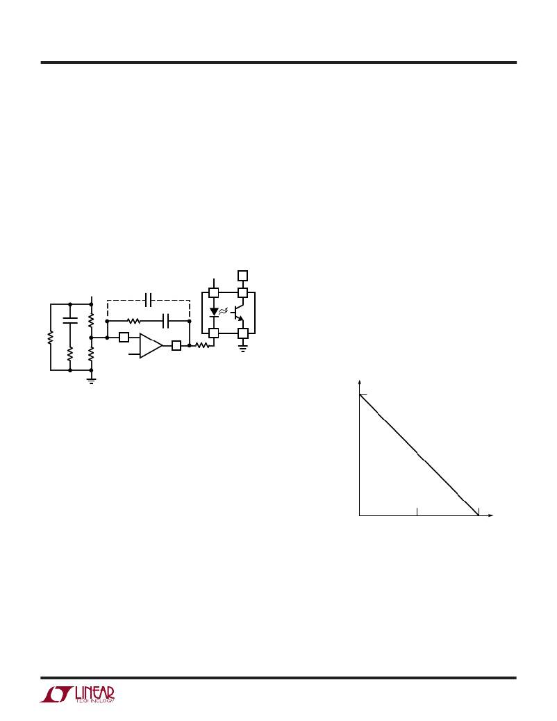
�Figure� 12.� Compensation� for� Polymer� Electrolytic�
�Aluminum� Electrolytic� (see� Figure� 12)� the� goal� of� this�
�compensator� will� be� to� cross� over� the� output� minimum�
�pole� frequency.� Set� a� low� frequency� pole� with� C� C� and� R� IN�
�at� a� frequency� that� will� cross� over� the� loop� at� the� output�
�pole� minimum� F,� place� the� zero� formed� by� C� C� and� R� f� at� the�
�output� pole� F.�
�Synchronous� Rectification�
�NORMALIZED�
�OUTPUT� RIPPLE�
�CURRENT�
�ATTENUATION�
�1�
�NOTE:� INDUCTOR(S)� DUTY� CYCLE�
�IS� LIMITED� TO� 50%� WITH� CURRENT�
�DOUBLER� PHASE� SHIFT� CONTROL.�
�The� LTC1922-1� produces� the� precise� timing� signals� nec-�
�essary� to� control� current� doubler� secondary� side� synchro-�
�0�
�0�
�0.25�
�DUTY� CYCLE�
�0.5�
�1922� ?� F13�
�nous� MOSFETs� on� OUTE� and� OUTF.� Synchronous� rectifi-�
�ers� are� used� in� place� of� Schottky� or� Silicon� diodes� on� the�
�secondary� side� of� the� power� supply.� As� MOSFET� R� DS(ON)�
�levels� continue� to� drop,� significant� efficiency� improve-�
�ments� can� be� realized� with� synchronous� rectification,�
�provided� that� the� MOSFET� switch� timing� is� optimized.� An�
�additional� benefit� realized� with� synchronous� rectifiers� is�
�bipolar� output� current� capability.� These� characteristics�
�improve� transient� response,� particularly� overshoot,� and�
�improve� ZVS� ability� at� light� loads.�
�Figure� 13.� Ripple� Current� Cancellation� vs� Duty� Cycle�
�Synchronous� rectification� of� the� current� doubler� second-�
�ary� requires� two� ground� referenced� N-channel� MOSFETs.�
�The� timing� of� the� LTC1922-1� drive� signals� is� shown� in� the�
�Timing� Diagram.� Synchronous� rectifier� turn-on� is� inter-�
�nally� delayed� by� the� LTC1922-1� after� OUT� (C� or� D)�
�turn-off—just� after� the� end� of� a� power� cycle.� Synchronous�
�rectifier� turn-off� occurs� coincident� with� OUT� (A� or� B)�
�turn-off.� This� gives� a� passive� transition� time� margin� before�
�21�
�相关PDF资料 |
PDF描述 |
|---|---|
| VE-21Y-EU-F2 | CONVERTER MOD DC/DC 3.3V 132W |
| LTC1437ACG#PBF | IC REG CTRLR BUCK PWM CM 28-SSOP |
| B43086A4476M | 47UF 350V 16X25 SINGLE END |
| RMC18DRYH | CONN EDGECARD 36POS DIP .100 SLD |
| H2AXG-10105-Y4-ND | JUMPER-H1503TR/A2015Y/X 5" |
相关代理商/技术参数 |
参数描述 |
|---|---|
| LTC1922IG-1 | 功能描述:IC REG CTRLR ISO PWM 20-SSOP RoHS:否 类别:集成电路 (IC) >> PMIC - 稳压器 - DC DC 切换控制器 系列:- 标准包装:4,500 系列:PowerWise® PWM 型:控制器 输出数:1 频率 - 最大:1MHz 占空比:95% 电源电压:2.8 V ~ 5.5 V 降压:是 升压:无 回扫:无 反相:无 倍增器:无 除法器:无 Cuk:无 隔离:无 工作温度:-40°C ~ 125°C 封装/外壳:6-WDFN 裸露焊盘 包装:带卷 (TR) 配用:LM1771EVAL-ND - BOARD EVALUATION LM1771 其它名称:LM1771SSDX |
| LTC1922IG-1#PBF | 功能描述:IC REG CTRLR ISO PWM 20-SSOP RoHS:是 类别:集成电路 (IC) >> PMIC - 稳压器 - DC DC 切换控制器 系列:- 标准包装:4,500 系列:PowerWise® PWM 型:控制器 输出数:1 频率 - 最大:1MHz 占空比:95% 电源电压:2.8 V ~ 5.5 V 降压:是 升压:无 回扫:无 反相:无 倍增器:无 除法器:无 Cuk:无 隔离:无 工作温度:-40°C ~ 125°C 封装/外壳:6-WDFN 裸露焊盘 包装:带卷 (TR) 配用:LM1771EVAL-ND - BOARD EVALUATION LM1771 其它名称:LM1771SSDX |
| LTC1922IG-1#TR | 功能描述:IC REG CTRLR ISO PWM 20-SSOP RoHS:否 类别:集成电路 (IC) >> PMIC - 稳压器 - DC DC 切换控制器 系列:- 标准包装:4,500 系列:PowerWise® PWM 型:控制器 输出数:1 频率 - 最大:1MHz 占空比:95% 电源电压:2.8 V ~ 5.5 V 降压:是 升压:无 回扫:无 反相:无 倍增器:无 除法器:无 Cuk:无 隔离:无 工作温度:-40°C ~ 125°C 封装/外壳:6-WDFN 裸露焊盘 包装:带卷 (TR) 配用:LM1771EVAL-ND - BOARD EVALUATION LM1771 其它名称:LM1771SSDX |
| LTC1922IG-1#TRPBF | 功能描述:IC REG CTRLR ISO PWM 20-SSOP RoHS:是 类别:集成电路 (IC) >> PMIC - 稳压器 - DC DC 切换控制器 系列:- 标准包装:4,500 系列:PowerWise® PWM 型:控制器 输出数:1 频率 - 最大:1MHz 占空比:95% 电源电压:2.8 V ~ 5.5 V 降压:是 升压:无 回扫:无 反相:无 倍增器:无 除法器:无 Cuk:无 隔离:无 工作温度:-40°C ~ 125°C 封装/外壳:6-WDFN 裸露焊盘 包装:带卷 (TR) 配用:LM1771EVAL-ND - BOARD EVALUATION LM1771 其它名称:LM1771SSDX |
| LTC1922IN-1 | 功能描述:IC REG CTRLR ISO PWM CM/VM 20DIP RoHS:否 类别:集成电路 (IC) >> PMIC - 稳压器 - DC DC 切换控制器 系列:- 标准包装:4,500 系列:PowerWise® PWM 型:控制器 输出数:1 频率 - 最大:1MHz 占空比:95% 电源电压:2.8 V ~ 5.5 V 降压:是 升压:无 回扫:无 反相:无 倍增器:无 除法器:无 Cuk:无 隔离:无 工作温度:-40°C ~ 125°C 封装/外壳:6-WDFN 裸露焊盘 包装:带卷 (TR) 配用:LM1771EVAL-ND - BOARD EVALUATION LM1771 其它名称:LM1771SSDX |
发布紧急采购,3分钟左右您将得到回复。