- 您现在的位置:买卖IC网 > PDF目录15286 > LTC1929CG-PG#TRPBF (Linear Technology)IC REG CTRLR BUCK PWM CM 28-SSOP PDF资料下载
参数资料
| 型号: | LTC1929CG-PG#TRPBF |
| 厂商: | Linear Technology |
| 文件页数: | 14/28页 |
| 文件大小: | 0K |
| 描述: | IC REG CTRLR BUCK PWM CM 28-SSOP |
| 标准包装: | 2,000 |
| PWM 型: | 电流模式 |
| 输出数: | 1 |
| 频率 - 最大: | 360kHz |
| 占空比: | 99.5% |
| 电源电压: | 4 V ~ 36 V |
| 降压: | 是 |
| 升压: | 无 |
| 回扫: | 无 |
| 反相: | 无 |
| 倍增器: | 无 |
| 除法器: | 无 |
| Cuk: | 无 |
| 隔离: | 无 |
| 工作温度: | 0°C ~ 85°C |
| 封装/外壳: | 28-SSOP(0.209",5.30mm 宽) |
| 包装: | 带卷 (TR) |
第1页第2页第3页第4页第5页第6页第7页第8页第9页第10页第11页第12页第13页当前第14页第15页第16页第17页第18页第19页第20页第21页第22页第23页第24页第25页第26页第27页第28页
�� �
�
�LTC1929/LTC1929-PG�
�APPLICATIO� S� I� FOR� ATIO�
�synchronous� MOSFET� losses� are� greatest� at� high� input�
�voltage� when� the� top� switch� duty� factor� is� low� or� during� a�
�short-circuit� when� the� synchronous� switch� is� on� close� to�
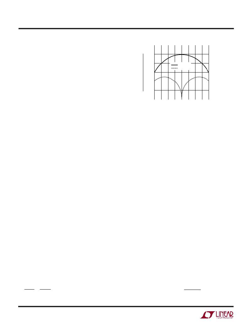
�0.6�
�0.5�
�100%� of� the� period.�
�The� term� (1� +� δ� )� is� generally� given� for� a� MOSFET� in� the�
�form� of� a� normalized� R� DS(ON)� vs.� Temperature� curve,� but�
�δ� =� 0.005/� °� C� can� be� used� as� an� approximation� for� low�
�voltage� MOSFETs.� C� RSS� is� usually� specified� in� the� MOS-�
�FET� characteristics.� The� constant� k� =� 1.7� can� be� used� to�
�0.4�
�0.3�
�0.2�
�0.1�
�1-PHASE�
�2-PHASE�
�estimate� the� contributions� of� the� two� terms� in� the� main�
�0�
�0.1�
�0.2�
�0.3� 0.4� 0.5� 0.6� 0.7�
�0.8�
�0.9�
�switch� dissipation� equation.�
�DUTY� FACTOR� (V� OUT� /V� IN� )�
�1929� F04�
�The� Schottky� diodes,� D1� and� D2� shown� in� Figure� 1� conduct�
�during� the� dead-time� between� the� conduction� of� the� two�
�large� power� MOSFETs.� This� helps� prevent� the� body� diode�
�of� the� bottom� MOSFET� from� turning� on,� storing� charge�
�during� the� dead-time,� and� requiring� a� reverse� recovery�
�period� which� would� reduce� efficiency.� A� 1A� to� 3A� (depend-�
�ing� on� output� current)� Schottky� diode� is� generally� a� good�
�compromise� for� both� regions� of� operation� due� to� the�
�relatively� small� average� current.� Larger� diodes� result� in�
�additional� transition� losses� due� to� their� larger� junction�
�capacitance.�
�C� IN� and� C� OUT� Selection�
�In� continuous� mode,� the� source� current� of� each� top�
�N-channel� MOSFET� is� a� square� wave� of� duty� cycle� V� OUT� /�
�V� IN� .� A� low� ESR� input� capacitor� sized� for� the� maximum�
�RMS� current� must� be� used.� The� details� of� a� close� form�
�equation� can� be� found� in� Application� Note� 77.� Figure� 4�
�shows� the� input� capacitor� ripple� current� for� a� 2-phase�
�configuration� with� the� output� voltage� fixed� and� input�
�voltage� varied.� The� input� ripple� current� is� normalized�
�against� the� DC� output� current.� The� graph� can� be� used� in�
�place� of� tedious� calculations.� The� minimum� input� ripple�
�current� can� be� achieved� when� the� input� voltage� is� twice� the�
�output� voltage.� The� minimum� is� not� quite� zero� due� to�
�inductor� ripple� current.�
�In� the� graph� of� Figure� 4,� the� local� maximum� input� RMS�
�capacitor� currents� are� reached� when:�
�Figure� 4.� Normalized� RMS� Input� Ripple� Current�
�vs� Duty� Factor� for� 1� and� 2� Output� Stages�
�These� worst-case� conditions� are� commonly� used� for� de-�
�sign� because� even� significant� deviations� do� not� offer� much�
�relief.� Note� that� capacitor� manufacturer’s� ripple� current�
�ratings� are� often� based� on� only� 2000� hours� of� life.� This�
�makes� it� advisable� to� further� derate� the� capacitor,� or� to�
�choose� a� capacitor� rated� at� a� higher� temperature� than�
�required.� Several� capacitors� may� also� be� paralleled� to� meet�
�size� or� height� requirements� in� the� design.� Always� consult�
�the� capacitor� manufacturer� if� there� is� any� question.�
�It� is� important� to� note� that� the� efficiency� loss� is� propor-�
�tional� to� the� input� RMS� current� squared� and� therefore� a�
�2-stage� implementation� results� in� 75%� less� power� loss�
�when� compared� to� a� single� phase� design.� Battery/input�
�protection� fuse� resistance� (if� used),� PC� board� trace� and�
�connector� resistance� losses� are� also� reduced� by� the� re-�
�duction� of� the� input� ripple� current� in� a� 2-phase� system.� The�
�required� amount� of� input� capacitance� is� further� reduced� by�
�the� factor,� 2,� due� to� the� effective� increase� in� the� frequency�
�of� the� current� pulses.�
�The� selection� of� C� OUT� is� driven� by� the� required� effective�
�series� resistance� (ESR).� Typically� once� the� ESR� require-�
�ment� has� been� met,� the� RMS� current� rating� generally� far�
�exceeds� the� I� RIPPLE(P-P)� requirements.� The� steady� state�
�output� ripple� (� ?� V� OUT� )� is� determined� by:�
�?� V� OUT� RIPPLE� ?� ESR� +�
�16� fC� OUT� ?�
�V� OUT�
�V� IN�
�=�
�2� k� ?� 1�
�4�
�where� k� =� 1,� 2.�
�≈� ?� I�
�?�
�?�
�1� ?�
�?�
�14�
�相关PDF资料 |
PDF描述 |
|---|---|
| VI-B2Z-EX-F1 | CONVERTER MOD DC/DC 2V 30W |
| VI-B2Z-EW-F4 | CONVERTER MOD DC/DC 2V 40W |
| VI-B2Z-EW-F2 | CONVERTER MOD DC/DC 2V 40W |
| VI-B2Z-EW-F1 | CONVERTER MOD DC/DC 2V 40W |
| VI-B2Y-EW-F2 | CONVERTER MOD DC/DC 3.3V 66W |
相关代理商/技术参数 |
参数描述 |
|---|---|
| LTC1929IG | 功能描述:IC REG CTRLR BUCK PWM CM 28-SSOP RoHS:否 类别:集成电路 (IC) >> PMIC - 稳压器 - DC DC 切换控制器 系列:- 标准包装:4,500 系列:PowerWise® PWM 型:控制器 输出数:1 频率 - 最大:1MHz 占空比:95% 电源电压:2.8 V ~ 5.5 V 降压:是 升压:无 回扫:无 反相:无 倍增器:无 除法器:无 Cuk:无 隔离:无 工作温度:-40°C ~ 125°C 封装/外壳:6-WDFN 裸露焊盘 包装:带卷 (TR) 配用:LM1771EVAL-ND - BOARD EVALUATION LM1771 其它名称:LM1771SSDX |
| LTC1929IG#PBF | 功能描述:IC REG CTRLR BUCK PWM CM 28-SSOP RoHS:是 类别:集成电路 (IC) >> PMIC - 稳压器 - DC DC 切换控制器 系列:- 标准包装:4,500 系列:PowerWise® PWM 型:控制器 输出数:1 频率 - 最大:1MHz 占空比:95% 电源电压:2.8 V ~ 5.5 V 降压:是 升压:无 回扫:无 反相:无 倍增器:无 除法器:无 Cuk:无 隔离:无 工作温度:-40°C ~ 125°C 封装/外壳:6-WDFN 裸露焊盘 包装:带卷 (TR) 配用:LM1771EVAL-ND - BOARD EVALUATION LM1771 其它名称:LM1771SSDX |
| LTC1929IG#TR | 功能描述:IC REG CTRLR BUCK PWM CM 28-SSOP RoHS:否 类别:集成电路 (IC) >> PMIC - 稳压器 - DC DC 切换控制器 系列:- 标准包装:4,500 系列:PowerWise® PWM 型:控制器 输出数:1 频率 - 最大:1MHz 占空比:95% 电源电压:2.8 V ~ 5.5 V 降压:是 升压:无 回扫:无 反相:无 倍增器:无 除法器:无 Cuk:无 隔离:无 工作温度:-40°C ~ 125°C 封装/外壳:6-WDFN 裸露焊盘 包装:带卷 (TR) 配用:LM1771EVAL-ND - BOARD EVALUATION LM1771 其它名称:LM1771SSDX |
| LTC1929IG#TRPBF | 功能描述:IC REG CTRLR BUCK PWM CM 28-SSOP RoHS:是 类别:集成电路 (IC) >> PMIC - 稳压器 - DC DC 切换控制器 系列:- 标准包装:4,500 系列:PowerWise® PWM 型:控制器 输出数:1 频率 - 最大:1MHz 占空比:95% 电源电压:2.8 V ~ 5.5 V 降压:是 升压:无 回扫:无 反相:无 倍增器:无 除法器:无 Cuk:无 隔离:无 工作温度:-40°C ~ 125°C 封装/外壳:6-WDFN 裸露焊盘 包装:带卷 (TR) 配用:LM1771EVAL-ND - BOARD EVALUATION LM1771 其它名称:LM1771SSDX |
| LTC1929IG-PG | 功能描述:IC REG CTRLR BUCK PWM CM 28-SSOP RoHS:否 类别:集成电路 (IC) >> PMIC - 稳压器 - DC DC 切换控制器 系列:- 标准包装:4,500 系列:PowerWise® PWM 型:控制器 输出数:1 频率 - 最大:1MHz 占空比:95% 电源电压:2.8 V ~ 5.5 V 降压:是 升压:无 回扫:无 反相:无 倍增器:无 除法器:无 Cuk:无 隔离:无 工作温度:-40°C ~ 125°C 封装/外壳:6-WDFN 裸露焊盘 包装:带卷 (TR) 配用:LM1771EVAL-ND - BOARD EVALUATION LM1771 其它名称:LM1771SSDX |
发布紧急采购,3分钟左右您将得到回复。