- 您现在的位置:买卖IC网 > PDF目录1934 > LTC1955IUH#TRPBF (Linear Technology)IC SMART CARD INTERFACE DL 32QFN PDF资料下载
参数资料
| 型号: | LTC1955IUH#TRPBF |
| 厂商: | Linear Technology |
| 文件页数: | 9/22页 |
| 文件大小: | 0K |
| 描述: | IC SMART CARD INTERFACE DL 32QFN |
| 标准包装: | 2,500 |
| 控制器类型: | 智能卡接口 |
| 接口: | 4 线串行 |
| 电源电压: | 1.7 V ~ 5.5 V |
| 电流 - 电源: | 10µA |
| 工作温度: | -40°C ~ 85°C |
| 安装类型: | 表面贴装 |
| 封装/外壳: | 32-WFQFN 裸露焊盘 |
| 供应商设备封装: | 32-QFN 裸露焊盘(5x5) |
| 包装: | 带卷 (TR) |
LTC1955
17
1955fd
For more information www.linear.com/LTC1955
DVCC and VBATT when in shutdown. For applications that
require virtually zero shutdown current, the DVCC pin can
be grounded. This will reduce the VBATT current to well
under a single microampere. Internal logic ensures that
theLTC1955isinshutdownwhenDVCCisgrounded.Note,
however, that all of the logic signals that are referenced
to DVCC (DIN, SCLK, LD, DATA, RIN, SYNC, ASYNC and
NC/NO) will have to be at 0V as well, to prevent ESD diodes
to DVCC from being forward-biased.
Operation at Higher Supplies
If a 5.5V to 6V supply voltage is available, it is possible
to achieve some power savings by bypassing the charge
pump. The higher supply can be connected directly to the
CPO pin. As long as the voltage on CPO is higher than that
at which it ordinarily regulates (5.35V or 3.7V depending
on voltage selections), the charge pump’s oscillator will
not run. This configuration can give considerable power
savings since the charge pump is not being used.
A voltage source is still needed on both DVCC and SVBATT/
PVBATT in this configuration. Recall that DVCC sets the
logic reference level for all the control and smart card
communication pins. The voltage on SVBATT/PVBATT can
be any convenient level that meets the parameters in the
Electrical Characteristics table.
The 5.5V to 6V supply can be left permanently connected
to CPO, but there will be approximately 5A of current flow
into CPO when the LTC1955 is in shutdown.
Charge Pump Strength
UnderlowVBATTconditions,theamountofcurrentavailable
to the smart cards is limited by the charge pump.
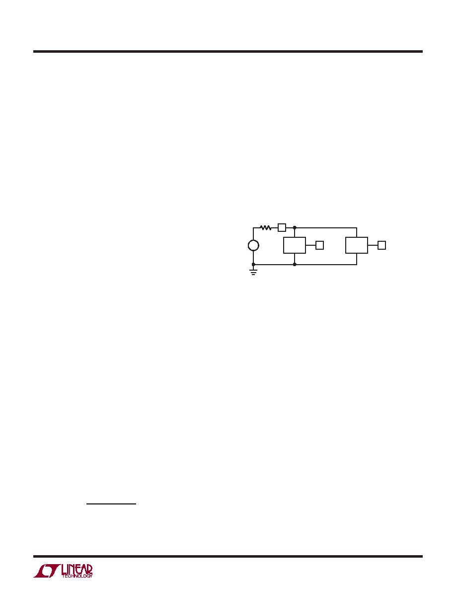
Figure 5 shows how the LTC1955 can be modeled as a
Thevenin equivalent circuit to determine the amount of
current available given the effective input voltage, 2VBATT
and the effective open-loop output resistance, ROLCP.
From Figure 5, the available current is given by:
ICCA +ICCB ≤
2VBATT – VCPO
ROLCP
ROLCP is dependent on a number of factors including the
switchingterm,1/(fOSCCFLY),internalswitchresistances
and the nonoverlap period of the switching circuit. How-
ever, for a given ROLCP, the minimum CPO voltage can be
determined from the following expression:
VCPO ≥ 2VBATT – (ICCA + ICCB)ROLCP
The LDOs have been designed to meet all applicable smart
card standards for VCC with VCPO as low as 5.13V. Given
this information, trade-offs can be made by the user with
regard to total consumption (ICCA + ICCB) and minimum
supply voltage.
+–
LDO A
2VBATT
1955 F05
CPO
ROLCP
VCCA
LDO B
VCCB
Figure 5. Equivalent Open-Loop Circuit
Changing the Smart Card Supply Voltage
Although the LTC1955 control system will allow the smart
card voltage to be changed from one value to the next
without an interim power-down, this is not recommended.
When changing from a higher voltage to a lower voltage
there will generally not be a problem; however, changing
from a lower voltage to a higher voltage will result in both
an undervoltage condition and an overcurrent condition
on that channel. The likely result is that the channel will
automatically deactivate. Applicable smart card standards
specify that the smart card supply be powered to zero
before applying a new voltage.
Compliance Testing
Inductance due to long leads on type approval equipment
can cause ringing and overshoot that leads to testing
problems. Small amounts of capacitance and damp-
ing resistors can be included in the application without
compromising the normal electrical performance of the
LTC1955 or smart card system. Generally, a 100Ω resis-
tor and a 20pF capacitor will accomplish this, as shown
in Figure 8.
applicaTions inForMaTion
相关PDF资料 |
PDF描述 |
|---|---|
| LTC202CS#TRPBF | IC SWITCH QUAD SPST 16SOIC |
| LTC221CN#PBF | IC SWITCH QUAD SPST 16DIP |
| LTC2801CDE#PBF | IC TXRX RS232 12-DFN |
| LTC2845IUHF#TRPBF | IC TXRX 3.3V MULTIPROTOCOL 38QFN |
| LTC2846IG#TRPBF | IC TXRX 3.3V MULTIPROTCOL 36SSOP |
相关代理商/技术参数 |
参数描述 |
|---|---|
| LTC1957-1EMS8 | 功能描述:IC RF PWR CONTRLLR SINGLE 8-MSOP RoHS:否 类别:RF/IF 和 RFID >> RF 电源控制器 IC 系列:- 标准包装:3,000 系列:- RF 型:GSM 频率:450MHz ~ 2GHz 特点:四频带 封装/外壳:8-VFBGA 供应商设备封装:8-MicroSMD(1.51x1.51) 包装:带卷 (TR) 其它名称:LMV243BLX |
| LTC1957-1EMS8#PBF | 功能描述:IC RF PWR CONTRLLR SINGLE 8-MSOP RoHS:是 类别:RF/IF 和 RFID >> RF 电源控制器 IC 系列:- 标准包装:3,000 系列:- RF 型:GSM 频率:450MHz ~ 2GHz 特点:四频带 封装/外壳:8-VFBGA 供应商设备封装:8-MicroSMD(1.51x1.51) 包装:带卷 (TR) 其它名称:LMV243BLX |
| LTC1957-1EMS8#TR | 功能描述:IC RF PWR CONTRLLR SINGLE 8-MSOP RoHS:否 类别:RF/IF 和 RFID >> RF 电源控制器 IC 系列:- 标准包装:3,000 系列:- RF 型:GSM 频率:450MHz ~ 2GHz 特点:四频带 封装/外壳:8-VFBGA 供应商设备封装:8-MicroSMD(1.51x1.51) 包装:带卷 (TR) 其它名称:LMV243BLX |
| LTC1957-1EMS8#TRPBF | 功能描述:IC RF PWR CONTRLLR SINGLE 8-MSOP RoHS:是 类别:RF/IF 和 RFID >> RF 电源控制器 IC 系列:- 标准包装:3,000 系列:- RF 型:GSM 频率:450MHz ~ 2GHz 特点:四频带 封装/外壳:8-VFBGA 供应商设备封装:8-MicroSMD(1.51x1.51) 包装:带卷 (TR) 其它名称:LMV243BLX |
| LTC1957-2EMS | 功能描述:IC RF PWR CONTROLLR DUAL 10-MSOP RoHS:否 类别:RF/IF 和 RFID >> RF 电源控制器 IC 系列:- 标准包装:3,000 系列:- RF 型:GSM 频率:450MHz ~ 2GHz 特点:四频带 封装/外壳:8-VFBGA 供应商设备封装:8-MicroSMD(1.51x1.51) 包装:带卷 (TR) 其它名称:LMV243BLX |
发布紧急采购,3分钟左右您将得到回复。