- 您现在的位置:买卖IC网 > PDF目录22183 > LTC1966CMS8#TR (Linear Technology)IC PREC RMS/DC CONV MCRPWR 8MSOP PDF资料下载
参数资料
| 型号: | LTC1966CMS8#TR |
| 厂商: | Linear Technology |
| 文件页数: | 4/38页 |
| 文件大小: | 391K |
| 描述: | IC PREC RMS/DC CONV MCRPWR 8MSOP |
| 标准包装: | 2,500 |
| 电流 - 电源: | 155µA |
| 电源电压: | 2.7 V ~ 5.5 V |
| 安装类型: | 表面贴装 |
| 封装/外壳: | 8-TSSOP,8-MSOP(0.118",3.00mm 宽) |
| 供应商设备封装: | 8-MSOP |
| 包装: | 带卷 (TR) |
| 其它名称: | LTC1966CMS8TR |
第1页第2页第3页当前第4页第5页第6页第7页第8页第9页第10页第11页第12页第13页第14页第15页第16页第17页第18页第19页第20页第21页第22页第23页第24页第25页第26页第27页第28页第29页第30页第31页第32页第33页第34页第35页第36页第37页第38页
LTC1966
4
1966fb
elecTrical characTerisTics
Note 1: Stresses beyond those listed under Absolute Maximum Ratings
may cause permanent damage to the device. Exposure to any Absolute
Maximum Rating condition for extended periods may affect device
reliability and lifetime.
Note 2: The inputs (IN1, IN2) are protected by shunt diodes to V
SS
and
V
DD
. If the inputs are driven beyond the rails, the current should be limited
to less than 10mA.
Note 3: The LTC1966 output (V
OUT
) is high impedance and can be
overdriven, either sinking or sourcing current, to the limits stated.
Note 4: The LTC1966C/LTC1966I are guaranteed functional over
the operating temperature range of 40癈 to 85癈. The LTC1966H/
LTC1966MP are guaranteed functional over the operating temperature
range of 55癈 to 125癈.
Note 5: The LTC1966C is guaranteed to meet specified performance from
0癈 to 70癈. The LTC1966C is designed, characterized and expected to
meet specified performance from 40癈 to 85癈 but is not tested nor
QA sampled at these temperatures. The LTC1966I is guaranteed to meet
specified performance from 40癈 to 85癈. The LTC1966H is guaranteed
to meet specified performance from 40癈 to 125癈. The LTC1966MP is
guaranteed to meet specified performance from 55癈 to 125癈.
Note 6: High speed automatic testing cannot be performed with
C
AVE
= 10礔. The LTC1966 is 100% tested with C
AVE
= 22nF. Correlation
tests have shown that the performance limits above can be guaranteed
with the additional testing being performed to guarantee proper operation
of all the internal circuitry.
Note 7: High speed automatic testing cannot be performed with 60Hz
inputs. The LTC1966 is 100% tested with DC and 10kHz input signals.
Measurements with DC inputs from 50mV to 350mV are used to calculate
the four parameters: G
ERR
, V
OOS
, V
IOS
and linearity error. Correlation tests
have shown that the performance limits above can be guaranteed with the
additional testing being performed to guarantee proper operation of all
internal circuitry.
Note 8: The LTC1966 is inherently very linear. Unlike older log/antilog
circuits, its behavior is the same with DC and AC inputs, and DC inputs are
used for high speed testing.
Note 9: The power supply rejections of the LTC1966 are measured with DC
inputs from 50mV to 350mV. The change in accuracy from V
DD
= 2.7V to
V
DD
= 5.5V with V
SS
= 0V is divided by 2.8V. The change in accuracy from
V
SS
= 0V to V
SS
= 5.5V with V
DD
= 5.5V is divided by 5.5V.
Note 10: Previous generation RMS-to-DC converters required nonlinear
input stages as well as a nonlinear core. Some parts specify a DC reversal
error, combining the effects of input nonlinearity and input offset voltage.
The LTC1966 behavior is simpler to characterize and the input offset
voltage is the only significant source of DC reversal error.
Note 11: High speed automatic testing cannot be performed with 60Hz
inputs. The LTC1966 is 100% tested with DC stimulus. Correlation tests
have shown that the performance limits above can be guaranteed with the
additional testing being performed to verify proper operation of all internal
circuitry.
Note 12: The LTC1966 is a switched capacitor device and the input/
output impedance is an average impedance over many clock cycles. The
input impedance will not necessarily lead to an attenuation of the input
signal measured. Refer to the Applications Information section titled Input
Impedance for more information.
Note 13: The common mode rejection ratios of the LTC1966 are measured
with DC inputs from 50mV to 350mV. The input CMRR is defined as the
change in V
IOS
measured between input levels of V
SS
to V
SS
+ 350mV and
input levels of V
DD
350mV to V
DD
divided by V
DD
V
SS
350mV. The
output CMRR is defined as the change in V
OOS
measured with OUT RTN =
V
SS
and OUT RTN = V
DD
350mV divided by V
DD
V
SS
350mV.
Note 14: Each input of the LTC1966 can withstand any voltage within
the supply range. These inputs are protected with ESD diodes, so going
beyond the supply voltages can damage the part if the absolute maximum
current ratings are exceeded. Likewise for the output pins. The LTC1966
input and output voltage swings are limited by internal clipping. The
maximum differential input of the LTC1966 (referred to as maximum input
swing) is 1V. This applies to either input polarity, so it can be thought of as
?V. Because the differential input voltage gets processed by the LTC1966
with gain, it is subject to internal clipping. Exceeding the 1V maximum
can, depending on the input crest factor, impact the accuracy of the output
voltage, but does not damage the part. Fortunately, the LTC1966s
topology is relatively tolerant of momentary internal clipping. The input
clipping is tested with a crest factor of 2, while the output clipping is
tested with a DC input.
Note 15: The LTC1966 exploits oversampling and noise shaping to reduce
the quantization noise of internal 1-bit analog-to-digital conversions. At
higher input frequencies, increasingly large portions of this noise are
aliased down to DC. Because the noise is shifted in frequency, it becomes
a low frequency rumble and is only filtered at the expense of increasingly
long settling times. The LTC1966 is inherently wideband, but the output
accuracy is degraded by this aliased noise. These specifications apply with
C
AVE
= 10礔 and constitute a 3-sigma variation of the output rumble.
Note 16: The LTC1966 can operate down to 2.7V single supply but cannot
operate at ?.7V. This additional constraint on V
SS
can be expressed
mathematically as 3 " (V
DD
2.7V) d V
SS
d Ground.
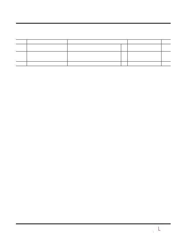
SYMBOL PARAMETER
CONDITIONS
MIN TYP MAX UNITS
I
IL
ENABLE Pin Current Low
V
ENABLE
= 0.5V
LTC1966H, LTC1966MP
l
l
2
10
1 0.1
礎
礎
V
TH
ENABLE Threshold Voltage
V
DD
= 5V, V
SS
= 5V
V
DD
= 5V, V
SS
= GND
V
DD
= 2.7V, V
SS
= GND
2.4
2.1
1.3
V
V
V
V
HYS
ENABLE Threshold Hysteresis
0.1
V
The l denotes the specifications which apply over the full operating
temperature range, otherwise specifications are at T
A
= 25癈. V
DD
= 5V, V
SS
= 5V, V
OUTRTN
= 0V, C
AVE
= 10礔, V
IN
= 200mV
RMS
,
V
ENABLE
= 0.5V unless otherwise noted.
相关PDF资料 |
PDF描述 |
|---|---|
| LTC1966CMS8 | IC PREC RMS/DC CONV MCRPWR 8MSOP |
| GBB106DHHR-S621 | CONN EDGECARD 212POS .050 SOLDER |
| RAC15-24SB-E | CONV AC/DC 2A 6.5-18VIN 3.0-5.5V |
| PR1502G-T | DIODE FAST REC 1.5A 100V DO-15 |
| GBB106DHHR-S578 | CONN EDGECARD 212POS .050 SLD |
相关代理商/技术参数 |
参数描述 |
|---|---|
| LTC1966HMS8#PBF | 功能描述:IC RMS/DC CONV MICROPWR 8-MSOP RoHS:是 类别:集成电路 (IC) >> PMIC - RMS 至 DC 转换器 系列:- 标准包装:46 系列:- 电流 - 电源:1.2mA 电源电压:±18 V,36 V 安装类型:表面贴装 封装/外壳:16-SOIC(0.295",7.50mm 宽) 供应商设备封装:16-SOIC W 包装:管件 |
| LTC1966HMS8#TRPBF | 功能描述:IC RMS/DC CONV MICROPWR 8-MSOP RoHS:是 类别:集成电路 (IC) >> PMIC - RMS 至 DC 转换器 系列:- 标准包装:46 系列:- 电流 - 电源:1.2mA 电源电压:±18 V,36 V 安装类型:表面贴装 封装/外壳:16-SOIC(0.295",7.50mm 宽) 供应商设备封装:16-SOIC W 包装:管件 |
| LTC1966IMS8 | 功能描述:IC PREC RMS/DC CONV MCRPWR 8MSOP RoHS:否 类别:集成电路 (IC) >> PMIC - RMS 至 DC 转换器 系列:- 标准包装:46 系列:- 电流 - 电源:1.2mA 电源电压:±18 V,36 V 安装类型:表面贴装 封装/外壳:16-SOIC(0.295",7.50mm 宽) 供应商设备封装:16-SOIC W 包装:管件 |
| LTC1966IMS8#PBF | 功能描述:IC PREC RMS/DC CONV MCRPWR 8MSOP RoHS:是 类别:集成电路 (IC) >> PMIC - RMS 至 DC 转换器 系列:- 标准包装:46 系列:- 电流 - 电源:1.2mA 电源电压:±18 V,36 V 安装类型:表面贴装 封装/外壳:16-SOIC(0.295",7.50mm 宽) 供应商设备封装:16-SOIC W 包装:管件 |
| LTC1966IMS8#TR | 功能描述:IC PREC RMS/DC CONV MCRPWR 8MSOP RoHS:否 类别:集成电路 (IC) >> PMIC - RMS 至 DC 转换器 系列:- 标准包装:46 系列:- 电流 - 电源:1.2mA 电源电压:±18 V,36 V 安装类型:表面贴装 封装/外壳:16-SOIC(0.295",7.50mm 宽) 供应商设备封装:16-SOIC W 包装:管件 |
发布紧急采购,3分钟左右您将得到回复。