- 您现在的位置:买卖IC网 > PDF目录14192 > LTC1983ES6-5#TRPBF (Linear Technology)IC REG SWITCHD CAP INV -5V SOT23 PDF资料下载
参数资料
| 型号: | LTC1983ES6-5#TRPBF |
| 厂商: | Linear Technology |
| 文件页数: | 8/12页 |
| 文件大小: | 0K |
| 描述: | IC REG SWITCHD CAP INV -5V SOT23 |
| 标准包装: | 2,500 |
| 类型: | 切换式电容器(充电泵),反相 |
| 输出类型: | 固定 |
| 输出数: | 1 |
| 输出电压: | -5V |
| 输入电压: | 2.3 V ~ 5.5 V |
| PWM 型: | Burst Mode? |
| 频率 - 开关: | 900kHz |
| 电流 - 输出: | 100mA |
| 同步整流器: | 无 |
| 工作温度: | -40°C ~ 85°C |
| 安装类型: | 表面贴装 |
| 封装/外壳: | SOT-23-6 细型,TSOT-23-6 |
| 包装: | 带卷 (TR) |
| 供应商设备封装: | TSOT-23-6 |
�� �
�
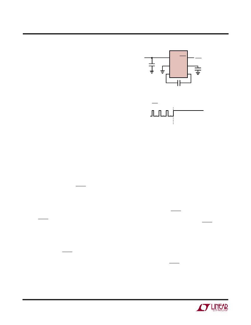
�LTC1983-3/LTC1983-5�
�OPERATIO�
�(Refer� to� Block� Diagram)�
�V� OUT�
�Inrush Currents�
�During� normal� operation,� V� IN� will� experience� current� tran-�
�sients� in� the� several� hundred� milliamp� range� whenever� the�
�charge� pump� is� enabled.� During� start-up,� these� inrush�
�currents� may� approach� 1� to� 2� amps.� For� this� reason,� it� is�
�V� IN�
�C� IN�
�10� μ� F�
�TANTALUM�
�3.3V� TO� 5.5V�
�LTC1983-3�
�V� IN� SHDN�
�GND�
�C� +� C� –�
�FROM� MPU�
�SHDN�
�–3V� ±� 4%�
�C� OUT�
�10� μ� F�
�CERAMIC�
�important� to� minimize� the� source� resistance� between� the�
�input� supply� and� the� V� IN� pin.� Too� much� source� resistance�
�may� result� in� regulation� problems� or� even� prevent� start-�
�up.� One� way� that� this� can� be� avoided� (especially� when� the�
�source� impedance� can’t� be� lowered� due� to� system� con-�
�straints)� is� to� use� a� large� V� IN� capacitor� with� low� ESR� right�
�C� FLY�
�1� μ� F�
�CERAMIC�
�SHDN� PIN� WAVEFORMS:�
�at� the� V� IN� pin.� If� ceramic� capacitors� are� used,� you� may�
�need� to� add� 1� μ� F� to� 10� μ� F� tantalum� capacitor� in� parallel� to�
�LOW� I� Q� MODE�
�(I� OUT� ≤� 100� μ� A)�
�V� OUT� LOAD� ENABLE� MODE�
�(I� OUT� =� 100� μ� A� TO� 100mA)�
�limit� input� voltage� transients.� Input� voltage� transients� will�
�occur� if� V� IN� is� applied� via� a� switch� or� a� plug.� One� example�
�(1Hz� TO� 100Hz,� 2%� TO� 5%� DUTY� CYCLE)�
�1983� F02�
�of� this� situation� is� in� USB� applications.�
�Ultralow� Quiescent� Current� Regulated� Supply�
�The� LTC1983� contains� an� internal� resistor� divider� (refer� to�
�the� Block� Diagram)� that� draws� only� 1� μ� A� (typ� for� the� 3V�
�version)� from� V� OUT� during� normal� operation.� During� shut-�
�down,� the� resistor� divider� is� disconnected� from� the� output�
�and� the� part� draws� only� leakage� current� from� the� output.�
�During� no-load� conditions,� applying� a� 1Hz� to� 100Hz,� 2%�
�to� 5%� duty� cycle� signal� to� the� SHDN� pin� ensures� that� the�
�circuit� of� Figure� 2� comes� out� of� shutdown� frequently�
�enough� to� maintain� regulation� even� under� low-load� condi-�
�tions.� Since� the� part� spends� nearly� all� of� its� time� in�
�shutdown,� the� no-load� quiescent� current� is� essentially�
�zero.� However,� the� part� will� still� be� in� operation� during� the�
�time� the� SHDN� pin� is� high,� so� the� current� will� not� be� zero�
�and� can� be� calculated� using� the� following� equations� to�
�determine� the� approximate� maximum� current:� I� IN(MAX)� =�
�[(Time� out� of� shutdown)� ?� (Burst� Mode� operation� quies-�
�cent� current)� +� (Normal� operating� I� IN� )� ?� (Time� output� is�
�being� charged� before� the� LTC1983� enters� Burst� Mode�
�operation)]/(Period� of� SHDN� signal).� This� number� will� be�
�highly� dependent� on� the� amount� of� board� leakage� current�
�and� how� many� devices� are� connected� to� V� OUT� (each� will�
�draw� some� leakage� current)� and� must� be� calculated� and�
�verified� for� each� different� board� design.�
�Figure� 2.� Ultralow� Quiescent� Current� Regulated� Supply�
�The� LTC1983� must� be� out� of� shutdown� for� a� minimum�
�duration� of� 200� μ� s� to� allow� enough� time� to� sense� the� output�
�and� keep� it� in� regulation.� A� 1Hz,� 2%� duty� cycle� signal� will�
�keep� V� OUT� in� regulation� under� no-load� conditions.� Even�
�though� the� term� no-load� is� used,� there� will� always� be� board�
�leakage� current� and� leakage� current� drawn� by� anything�
�connected� to� V� OUT� .� This� is� why� it� is� necessary� to� wake� the�
�part� up� every� once� in� a� while� to� verify� regulation.� As� the�
�V� OUT� load� current� increases,� the� frequency� with� which� the�
�part� is� taken� out� of� shutdown� must� also� be� increased� to�
�prevent� V� OUT� from� drooping� below� the� –� 2.88V� (for� the� 3V�
�version)� during� the� OFF� phase� (see� Figure� 3).� A� 100Hz,� 2%�
�duty� cycle� signal� on� the� SHDN� pin� ensures� proper� regula-�
�tion� with� load� currents� as� high� as� 100� μ� A.� When� load�
�current� greater� than� 100� μ� A� is� needed,� the� SHDN� pin� must�
�be� forced� high� as� in� normal� operation.�
�Each� time� the� LTC1983� comes� out� of� shutdown,� the� part�
�delivers� a� minimum� of� one� clock� cycle� worth� of� charge� to�
�the� output.� Under� high� V� IN� (>4V)� and/or� low� I� OUT� (<10� μ� A)�
�conditions,� this� behavior� may� cause� a� net� excess� of� charge�
�to� be� delivered� to� the� output� capacitor� if� a� high� frequency�
�signal� is� used� on� the� SHDN� pin� (e.g.,� 50Hz� to� 100Hz).�
�Under� such� conditions,� V� OUT� will� slowly� drift� positive� and�
�may� even� go� out� of� regulation.� To� avoid� this� potential�
�1983fa�
�8�
�相关PDF资料 |
PDF描述 |
|---|---|
| MAX6865UK46D1S+T | IC MPU SUPERVISOR SOT23-5 |
| GCB10DHBN | CONN EDGECARD 20POS R/A .050 SLD |
| MAX6865UK46D6S+T | IC MPU SUPERVISOR SOT23-5 |
| CGS264U016V5L | CAP ALUM 260000UF 16V SCREW |
| MAX6866UK16D1L+T | IC MPU SUPERVISOR SOT23-5 |
相关代理商/技术参数 |
参数描述 |
|---|---|
| LTC1985ES5-1.8 | 制造商:Linear Technology 功能描述:Volt Supervisor Monitor 1.8V/3V 5-Pin TSOT-23 制造商:Linear Technology 功能描述:3-CHANNEL POWER SUPPLY SUPPORT CKT, PDSO5 |
| LTC1985ES5-1.8#PBF | 制造商:Linear Technology 功能描述:Volt Supervisor Monitor 1.8V/3V 5-Pin TSOT-23 制造商:Linear Technology 功能描述:MS-System Monitor/Supervisor, cut tape uP Triple Supply Monitor w Push-Pull |
| LTC1985ES5-1.8#TR | 功能描述:IC MON TRPL SUPPLY PREC TSOT23-5 RoHS:否 类别:集成电路 (IC) >> PMIC - 监控器 系列:- 标准包装:400 系列:- 类型:备用电池电路 监视电压数目:1 输出:开路漏极,推挽式 复位:高有效/低有效 复位超时:最小为 35 ms 电压 - 阀值:4.65V 工作温度:-40°C ~ 85°C 安装类型:表面贴装 封装/外壳:16-SOIC(0.295",7.50mm 宽) 供应商设备封装:16-SOIC W 包装:带卷 (TR) 其它名称:ADM691ARZ-REEL7TR |
| LTC1985ES5-1.8#TRM | 功能描述:IC MON TRI SUPPLY 1.8V TSOT23-5 RoHS:否 类别:集成电路 (IC) >> PMIC - 监控器 系列:- 标准包装:400 系列:- 类型:备用电池电路 监视电压数目:1 输出:开路漏极,推挽式 复位:高有效/低有效 复位超时:最小为 35 ms 电压 - 阀值:4.65V 工作温度:-40°C ~ 85°C 安装类型:表面贴装 封装/外壳:16-SOIC(0.295",7.50mm 宽) 供应商设备封装:16-SOIC W 包装:带卷 (TR) 其它名称:ADM691ARZ-REEL7TR |
| LTC1985ES5-1.8#TRMPBF | 功能描述:IC MON TRI SUPPLY 1.8V TSOT23-5 RoHS:是 类别:集成电路 (IC) >> PMIC - 监控器 系列:- 标准包装:400 系列:- 类型:备用电池电路 监视电压数目:1 输出:开路漏极,推挽式 复位:高有效/低有效 复位超时:最小为 35 ms 电压 - 阀值:4.65V 工作温度:-40°C ~ 85°C 安装类型:表面贴装 封装/外壳:16-SOIC(0.295",7.50mm 宽) 供应商设备封装:16-SOIC W 包装:带卷 (TR) 其它名称:ADM691ARZ-REEL7TR |
发布紧急采购,3分钟左右您将得到回复。