- 您现在的位置:买卖IC网 > PDF目录14217 > LTC1986ES6#TR (Linear Technology)IC REG BOOST SWITCHED CAP SOT23 PDF资料下载
参数资料
| 型号: | LTC1986ES6#TR |
| 厂商: | Linear Technology |
| 文件页数: | 5/8页 |
| 文件大小: | 0K |
| 描述: | IC REG BOOST SWITCHED CAP SOT23 |
| 标准包装: | 2,500 |
| 类型: | 升压(升压),切换电容(充电泵) |
| 输出类型: | 固定 |
| 输出数: | 1 |
| 输出电压: | 3V,5V |
| 输入电压: | 2.6 V ~ 4.4 V |
| 频率 - 开关: | 900kHz |
| 电流 - 输出: | 10mA |
| 同步整流器: | 无 |
| 工作温度: | -40°C ~ 85°C |
| 安装类型: | 表面贴装 |
| 封装/外壳: | SOT-23-6 细型,TSOT-23-6 |
| 包装: | 带卷 (TR) |
| 供应商设备封装: | TSOT-23-6 |
�� �
�
�LTC1986�
�APPLICATIO� N� S� I� N� FOR� M� ATIO� N�
�Operation�
�The� LTC1986� is� a� charge� pump� DC/DC� converter� designed�
�specifically� to� supply� V� CC� power� for� either� 3V� or� 5V� SIM�
�cards.� The� part� can� operate� in� one� of� three� modes:� a� low�
�power� shutdown� mode� which� disconnects� V� IN� from� V� OUT�
�and� actively� pulls� down� the� V� OUT� supply,� 3V� mode� which�
�provides� a� direct� connection� between� V� IN� and� V� OUT� for�
�powering� 3V� SIM� cards,� and� 5V� mode� which� provides� a�
�regulated� 5V� output� for� powering� 5V� SIM� cards.� In� 5V�
�mode,� regulation� is� achieved� by� sensing� the� output� volt-�
�age� through� a� resistor� divider� and� enabling� the� charge�
�pump� as� needed� to� maintain� regulation.�
�When� the� charge� pump� is� enabled,� a� 2-phase�
�nonoverlapping� clock� controls� the� internal� charge� pump�
�switches.� Flying� capacitor� C1� is� charged� to� V� IN� on� phase�
�one� of� the� clock.� On� phase� two� of� the� clock,� C1� is� stacked�
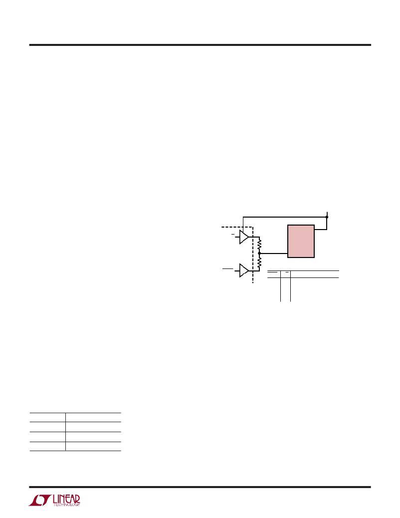
�The� three� modes� can� be� selected� using� two� totem� pole�
�digital� outputs� and� two� external� resistors� as� shown� in�
�Figure� 1.�
�Shutdown� mode� disconnects� V� IN� from� V� OUT� and� enables�
�an� internal� pull-down� device� which� forces� V� OUT� to� GND.�
�To� achieve� the� lowest� possible� quiescent� current� in� shut-�
�down� mode,� the� voltage� on� the� MODE� pin� should� be� pulled�
�below� 0.4V.� 3V� mode� connects� V� OUT� to� V� IN� through� a� 2.5� ?�
�internal� switch.� The� LTC1986� has� the� additional� capability�
�of� boosting� V� OUT� to� a� regulated� 2.9V� in� 3V� mode� when� the�
�input� voltage� drops� below� 2.85V.� This� ensures� that� the� 3V�
�SIM� V� CC� specification� is� not� violated� if� V� IN� drops� below�
�2.7V� during� transients� or� low� battery� conditions.�
�V� IN�
�in� series� with� V� IN� and� connected� to� V� OUT� through� an�
�V� IN�
�6�
�internal� switch.� This� sequence� of� charging� and� discharg-�
�ing� the� flying� capacitor� occurs� at� a� free-running� frequency�
�of� 900kHz� (typ)� and� continues� until� the� divided� output�
�3/5�
�1M�
�3�
�LTC1986�
�MODE�
�voltage� reaches� the� upper� trip� point� of� the� comparator.�
�750k�
�Once� the� output� is� in� regulation,� the� charge� pump� is�
�SHDN�
�SHDN� 3/5�
�MODE�
�disabled.� This� method� of� bursting� the� charge� pump� on� and�
�off� enables� the� LTC1986� to� achieve� high� efficiency� at�
�extremely� low� output� loads.�
�0�
�0�
�1�
�1�
�0�
�1�
�0�
�1�
�SHUTDOWN� (I� CC� <� 1� μ� A)�
�SHUTDOWN� (I� CC� =� 10� μ� A)�
�V� OUT� =� 5V�
�V� OUT� =� V� IN�
�1986� F01�
�Mode� Selection�
�The� operating� mode� is� determined� by� the� voltage� applied�
�to� the� MODE� pin.� The� MODE� pin� has� three� voltage� thresh-�
�olds—all� of� which� are� referenced� to� V� IN� :�
�Shutdown� Mode� ?� V� MODE� <� V� IN� /2� –� 0.1V�
�5V� Mode� ?� V� IN� /2� +� 0.1V� <� V� MODE� <� V� IN� –� 1V�
�3V� Mode� ?� V� IN� –� 0.25V� <� V� MODE�
�For� example,� if� V� IN� =� 3V,� then� the� following� table� applies:�
�Figure� 1�
�Capacitor� Selection�
�For� best� performance,� it� is� recommended� that� low� ESR�
�capacitors� be� used� for� both� C� IN� and� C� OUT� to� reduce� noise�
�and� ripple.� The� C� IN� and� C� OUT� capacitors� should� be� either�
�ceramic� or� tantalum.� Ceramic� capacitors� will� provide� the�
�smallest� size� for� a� given� capacitance.� If� the� input� source�
�impedance� is� very� low� (<� 0.5� ?� ),� C� IN� may� not� be� needed.�
�For� best� performance,� C� OUT� should� be� 2.2� μ� F� or� greater.�
�V� MODE�
�0V� to� 1.4V�
�1.6V� to� 2V�
�2.75V� to� 3V�
�OPERATING� MODE�
�Shutdown� Mode�
�5V� Mode�
�3V� Mode� (V� OUT� =� V� IN� )�
�Ceramic� capacitors� are� also� recommended� for� the� flying�
�capacitor� C1� with� values� between� 0.047� μ� F� and� 0.22� μ� F.� If�
�a� small� value� output� capacitor� (3.3� μ� F� or� less)� is� used,� a�
�small� flying� capacitor� should� also� be� used� to� prevent� high�
�output� ripple� in� 5V� mode.� The� recommended� capacitor�
�values� to� minimize� board� space� and� cost� are:� C� IN� =� 0.1� μ� F,�
�C1� =� 0.047� μ� F� and� C� OUT� =� 2.2� μ� F� (ceramic).�
�1986fa�
�5�
�相关PDF资料 |
PDF描述 |
|---|---|
| HM66A-0315100MLF13 | SHIELDED POWER INDUCTORS |
| EMC07DRYI-S93 | CONN EDGECARD 14POS DIP .100 SLD |
| SP7651ER-L/TR | IC REG BUCK SYNC ADJ 3A 26DFN |
| HM66A-03158R2NLF13 | SHIELDED POWER INDUCTORS |
| EEC31DRYI-S93 | CONN EDGECARD 62POS DIP .100 SLD |
相关代理商/技术参数 |
参数描述 |
|---|---|
| LTC1992-10CMS8 | 功能描述:IC AMP/DVR DIFF I/O GAIN10 8MSOP RoHS:否 类别:集成电路 (IC) >> Linear - Amplifiers - Instrumentation 系列:- 标准包装:73 系列:Over-The-Top® 放大器类型:通用 电路数:4 输出类型:满摆幅 转换速率:0.07 V/µs 增益带宽积:200kHz -3db带宽:- 电流 - 输入偏压:1nA 电压 - 输入偏移:285µV 电流 - 电源:50µA 电流 - 输出 / 通道:25mA 电压 - 电源,单路/双路(±):2 V ~ 44 V,±1 V ~ 22 V 工作温度:-40°C ~ 85°C 安装类型:表面贴装 封装/外壳:16-WFDFN 裸露焊盘 供应商设备封装:16-DFN-EP(5x3) 包装:管件 |
| LTC1992-10CMS8#PBF | 功能描述:IC AMP/DVR DIFF I/O GAIN10 8MSOP RoHS:是 类别:集成电路 (IC) >> Linear - Amplifiers - Instrumentation 系列:- 标准包装:73 系列:Over-The-Top® 放大器类型:通用 电路数:4 输出类型:满摆幅 转换速率:0.07 V/µs 增益带宽积:200kHz -3db带宽:- 电流 - 输入偏压:1nA 电压 - 输入偏移:285µV 电流 - 电源:50µA 电流 - 输出 / 通道:25mA 电压 - 电源,单路/双路(±):2 V ~ 44 V,±1 V ~ 22 V 工作温度:-40°C ~ 85°C 安装类型:表面贴装 封装/外壳:16-WFDFN 裸露焊盘 供应商设备封装:16-DFN-EP(5x3) 包装:管件 |
| LTC1992-10CMS8#TR | 功能描述:IC AMP/DVR DIFF I/O GAIN10 8MSOP RoHS:否 类别:集成电路 (IC) >> Linear - Amplifiers - Instrumentation 系列:- 标准包装:73 系列:Over-The-Top® 放大器类型:通用 电路数:4 输出类型:满摆幅 转换速率:0.07 V/µs 增益带宽积:200kHz -3db带宽:- 电流 - 输入偏压:1nA 电压 - 输入偏移:285µV 电流 - 电源:50µA 电流 - 输出 / 通道:25mA 电压 - 电源,单路/双路(±):2 V ~ 44 V,±1 V ~ 22 V 工作温度:-40°C ~ 85°C 安装类型:表面贴装 封装/外壳:16-WFDFN 裸露焊盘 供应商设备封装:16-DFN-EP(5x3) 包装:管件 |
| LTC1992-10CMS8#TRPBF | 功能描述:IC AMP/DVR DIFF I/O GAIN10 8MSOP RoHS:是 类别:集成电路 (IC) >> Linear - Amplifiers - Instrumentation 系列:- 标准包装:73 系列:Over-The-Top® 放大器类型:通用 电路数:4 输出类型:满摆幅 转换速率:0.07 V/µs 增益带宽积:200kHz -3db带宽:- 电流 - 输入偏压:1nA 电压 - 输入偏移:285µV 电流 - 电源:50µA 电流 - 输出 / 通道:25mA 电压 - 电源,单路/双路(±):2 V ~ 44 V,±1 V ~ 22 V 工作温度:-40°C ~ 85°C 安装类型:表面贴装 封装/外壳:16-WFDFN 裸露焊盘 供应商设备封装:16-DFN-EP(5x3) 包装:管件 |
| LTC1992-10HMS8 | 功能描述:IC AMP/DVR DIFF I/O GAIN10 8MSOP RoHS:否 类别:集成电路 (IC) >> Linear - Amplifiers - Instrumentation 系列:- 标准包装:150 系列:- 放大器类型:音频 电路数:2 输出类型:- 转换速率:5 V/µs 增益带宽积:12MHz -3db带宽:- 电流 - 输入偏压:100nA 电压 - 输入偏移:500µV 电流 - 电源:6mA 电流 - 输出 / 通道:50mA 电压 - 电源,单路/双路(±):4 V ~ 32 V,±2 V ~ 16 V 工作温度:-40°C ~ 85°C 安装类型:表面贴装 封装/外壳:8-TSSOP(0.173",4.40mm 宽) 供应商设备封装:8-TSSOP 包装:管件 |
发布紧急采购,3分钟左右您将得到回复。