- 您现在的位置:买卖IC网 > PDF目录6053 > LTC2051IS8#PBF (Linear Technology)IC OP-AMP ZERO-DRIFT DUAL 8-SOIC PDF资料下载
参数资料
| 型号: | LTC2051IS8#PBF |
| 厂商: | Linear Technology |
| 文件页数: | 8/12页 |
| 文件大小: | 0K |
| 描述: | IC OP-AMP ZERO-DRIFT DUAL 8-SOIC |
| 标准包装: | 100 |
| 放大器类型: | 断路器(零漂移) |
| 电路数: | 2 |
| 输出类型: | 满摆幅 |
| 转换速率: | 2 V/µs |
| 增益带宽积: | 3MHz |
| 电流 - 输入偏压: | 25pA |
| 电压 - 输入偏移: | 0.5µV |
| 电流 - 电源: | 850µA |
| 电压 - 电源,单路/双路(±): | 2.7 V ~ 7 V |
| 工作温度: | -40°C ~ 85°C |
| 安装类型: | 表面贴装 |
| 封装/外壳: | 8-SOIC(0.154",3.90mm 宽) |
| 供应商设备封装: | 8-SO |
| 包装: | 管件 |
5
LTC2051/LTC2052
20512fd
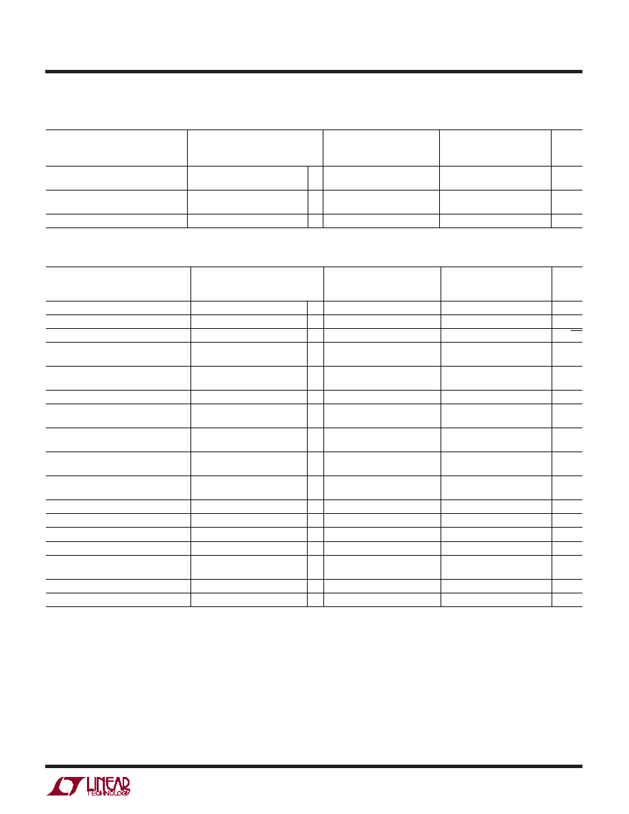
ELECTRICAL CHARACTERISTICS
LTC2051C/LTC2052C
LTC2051I/LTC2052I
LTC2051H/LTC2052H
PARAMETER
CONDITIONS
MIN
TYP
MAX
MIN
TYP
MAX
UNITS
(LTC2051/LTC2052, LTC2051HV/LTC2052HV) The
● denotes the
specifications which apply over the full operating temperature range, otherwise specifications are at TA = 25°C. VS = 3V, 5V
unless otherwise noted. (Note 3)
Shutdown Pin Input Low Voltage (VIL)
●
V – + 0.5
V
Shutdown Pin Input High Voltage (VIH)
●
V + – 0.5
V
Shutdown Pin Input Current
VSHDN = VIL, VS = 3V
●
–1
–3
–1
–3
μA
VSHDN = VIL, VS = 5V
●
–2
–5
–2
–5
μA
Internal Sampling Frequency
7.5
kHz
LTC2051C/LTC2052C
LTC2051I/LTC2052I
LTC2051H/LTC2052H
PARAMETER
CONDITIONS
MIN
TYP
MAX
MIN
TYP
MAX
UNITS
Input Offset Voltage
(Note 2)
±1
±3
±1
±3
μV
Average Input Offset Drift
(Note 2)
●
0.01
±0.03
0.01
±0.05
μV/°C
Long-Term Offset Drift
50
nV/√mo
Input Bias Current (Note 4)
±90
±150
±90
±150
pA
●
±300
±3000
pA
Input Offset Current (Note 4)
±300
pA
●
±500
±700
pA
Input Noise Voltage
RS = 100Ω, DC to 10Hz
1.5
μVP-P
Common Mode Rejection Ratio
VCM = V– to V+ – 1.3
125
130
125
130
dB
●
120
130
120
130
dB
Power Supply Rejection Ratio
120
130
120
130
dB
●
115
130
115
130
dB
Large-Signal Voltage Gain
RL = 10k
125
140
125
140
dB
●
120
140
120
140
dB
Maximum Output Voltage Swing
RL = 2k to GND
●
±4.75
±4.92
±4.50
±4.92
V
RL = 10k to GND
●
±4.90
±4.98
±4.85
±4.98
V
Slew Rate
22
V/μs
Gain Bandwidth Product
3
MHz
Supply Current (Per Amplifier)
No Load, VSHDN = VIH
●
1
1.5
1
1.5
mA
Supply Current, Shutdown
VSHDN = VIL
●
15
30
15
30
μA
Shutdown Pin Input Low Voltage (VIL)
●
V – + 0.5
V
Shutdown Pin Input High Voltage (VIH)
●
V + – 0.5
V
Shutdown Pin Input Current
VSHDN = VIL
●
–7
–15
– 7
– 15
μA
Internal Sampling Frequency
7.5
kHz
Note 1: Stresses beyond those listed under Absolute Maximum Ratings
may cause permanent damage to the device. Exposure to any Absolute
Maximum Rating condition for extended periods may affect device
reliability and lifetime.
Note 2: These parameters are guaranteed by design. Thermocouple effects
preclude measurements of these voltage levels during automated testing.
Note 3: All versions of the LTC2051/LTC2052 are designed, characterized
and expected to meet the extended temperature limits of – 40°C and 125°C.
The LTC2051C/LTC2052C/LTC2051HVC/LTC2052HVC are guaranteed to
meet the temperature limits of 0°C and 70°C. The LTC2051I/LTC2052I/
LTC2051HVI/LTC2052HVI are guaranteed to meet temperature limits of –
40°C and 85°C. The LTC2051H/LTC2051HVH and LTC2052H/LTC2052HVH
(LTC2051HV/LTC2052HV) The
● denotes the specifications which apply over the full operating temperature range, otherwise
specifications are at TA = 25°C. VS = ±5V unless otherwise noted. (Note 3)
are guaranteed to meet the temperature limits of – 40°C and 125°C.
Note 4: The bias current measurement accuracy depends on the proximity of
the negative supply bypass capacitors to the device under test. Because of
this, only the bias current of channel B (LTC2051) and channels A and B
(LTC2052) are 100% tested to the data sheet specifications. The bias
currents of the remaining channels are 100% tested to relaxed limits,
however, their values are guaranteed by design to meet the data sheet limits.
Note 5: This parameter is guaranteed to meet specified performance
through design and characterization. It has not been tested.
Note 6: The θJA specified for the DD package is with minimal PCB heat
spreading metal. Using expanded metal area on all layers of a board
reduces this value.
相关PDF资料 |
PDF描述 |
|---|---|
| 98414-G06-22LF | CONN HEADER 22POS 2MM STR DL PCB |
| PBC28SAAN | CONN HEADER .100 SINGL STR 28POS |
| D2540-6002-AR | CONN HEADER 40POS VERT 10GOLD |
| 159234-5002 | CONN HEADER 2MM 34POS R/A GOLD |
| 951136-7622-AR | CONN HEADER 36POS 2MM R/A T/H |
相关代理商/技术参数 |
参数描述 |
|---|---|
| LTC2052 | 制造商:LINER 制造商全称:Linear Technology 功能描述:High Voltage, High-Side Current Sense |
| LTC2052CGN | 功能描述:IC OPAMP ZERO-DRIFT QUAD 16SSOP RoHS:否 类别:集成电路 (IC) >> Linear - Amplifiers - Instrumentation 系列:- 标准包装:73 系列:Over-The-Top® 放大器类型:通用 电路数:4 输出类型:满摆幅 转换速率:0.07 V/µs 增益带宽积:200kHz -3db带宽:- 电流 - 输入偏压:1nA 电压 - 输入偏移:285µV 电流 - 电源:50µA 电流 - 输出 / 通道:25mA 电压 - 电源,单路/双路(±):2 V ~ 44 V,±1 V ~ 22 V 工作温度:-40°C ~ 85°C 安装类型:表面贴装 封装/外壳:16-WFDFN 裸露焊盘 供应商设备封装:16-DFN-EP(5x3) 包装:管件 |
| LTC2052CGN#PBF | 功能描述:IC OPAMP ZERO-DRIFT QUAD 16SSOP RoHS:是 类别:集成电路 (IC) >> Linear - Amplifiers - Instrumentation 系列:- 标准包装:2,500 系列:- 放大器类型:通用 电路数:4 输出类型:- 转换速率:0.6 V/µs 增益带宽积:1MHz -3db带宽:- 电流 - 输入偏压:45nA 电压 - 输入偏移:2000µV 电流 - 电源:1.4mA 电流 - 输出 / 通道:40mA 电压 - 电源,单路/双路(±):3 V ~ 32 V,±1.5 V ~ 16 V 工作温度:0°C ~ 70°C 安装类型:表面贴装 封装/外壳:14-TSSOP(0.173",4.40mm 宽) 供应商设备封装:14-TSSOP 包装:带卷 (TR) 其它名称:LM324ADTBR2G-NDLM324ADTBR2GOSTR |
| LTC2052CGN#TR | 功能描述:IC OPAMP ZERO-DRIFT QUAD 16SSOP RoHS:否 类别:集成电路 (IC) >> Linear - Amplifiers - Instrumentation 系列:- 标准包装:73 系列:Over-The-Top® 放大器类型:通用 电路数:4 输出类型:满摆幅 转换速率:0.07 V/µs 增益带宽积:200kHz -3db带宽:- 电流 - 输入偏压:1nA 电压 - 输入偏移:285µV 电流 - 电源:50µA 电流 - 输出 / 通道:25mA 电压 - 电源,单路/双路(±):2 V ~ 44 V,±1 V ~ 22 V 工作温度:-40°C ~ 85°C 安装类型:表面贴装 封装/外壳:16-WFDFN 裸露焊盘 供应商设备封装:16-DFN-EP(5x3) 包装:管件 |
| LTC2052CGN#TRPBF | 功能描述:IC OPAMP ZERO-DRIFT QUAD 16SSOP RoHS:是 类别:集成电路 (IC) >> Linear - Amplifiers - Instrumentation 系列:- 标准包装:73 系列:Over-The-Top® 放大器类型:通用 电路数:4 输出类型:满摆幅 转换速率:0.07 V/µs 增益带宽积:200kHz -3db带宽:- 电流 - 输入偏压:1nA 电压 - 输入偏移:285µV 电流 - 电源:50µA 电流 - 输出 / 通道:25mA 电压 - 电源,单路/双路(±):2 V ~ 44 V,±1 V ~ 22 V 工作温度:-40°C ~ 85°C 安装类型:表面贴装 封装/外壳:16-WFDFN 裸露焊盘 供应商设备封装:16-DFN-EP(5x3) 包装:管件 |
发布紧急采购,3分钟左右您将得到回复。