参数资料
| 型号: | LTC2053HDD |
| 厂商: | Linear Technology |
| 文件页数: | 2/18页 |
| 文件大小: | 0K |
| 描述: | IC AMP INST 0-DRFT R-R I/O 8-DFN |
| 标准包装: | 121 |
| 放大器类型: | 断路器(零漂移) |
| 电路数: | 1 |
| 输出类型: | 满摆幅 |
| 转换速率: | 0.2 V/µs |
| 增益带宽积: | 200kHz |
| 电流 - 输入偏压: | 4nA |
| 电压 - 输入偏移: | 5µV |
| 电流 - 电源: | 950µA |
| 电压 - 电源,单路/双路(±): | 2.7 V ~ 11 V,±1.35 V ~ 5.5 V |
| 工作温度: | -40°C ~ 125°C |
| 安装类型: | 表面贴装 |
| 封装/外壳: | 8-WFDFN 裸露焊盘 |
| 供应商设备封装: | 8-DFN-EP(3x3) |
| 包装: | 管件 |
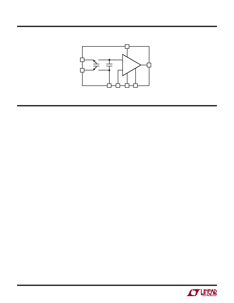
LTC2053/LTC2053-SYNC
0
2053syncfc
block DiagraM
–
+
ZERO-DRIFT
OP AMP
CH
OUT
2053 BD
4
V–
5
REF
6
RG
8
V+
1
EN/CLK*
3
+IN
2
–IN
CS
7
*NOTE: PIN 1 IS EN ON THE LTC2053 AND CLK ON THE LTC2053-SYNC
applicaTions inForMaTion
Theory of Operation
The LTC2053 uses an internal capacitor (CS) to sample
a differential input signal riding on a DC common mode
voltage (see the Block Diagram). This capacitor’s charge is
transferred to a second internal hold capacitor (CH) trans-
lating the common mode of the input differential signal to
that of the REF pin. The resulting signal is amplified by a
zero-drift op amp in the noninverting configuration. The
RG pin is the negative input of this op amp and allows
external programmability of the DC gain. Simple filtering
can be realized by using an external capacitor across the
feedback resistor.
Input Voltage Range
The input common mode voltage range of the LTC2053
is rail-to-rail. However, the following equation limits the
size of the differential input voltage:
V– ≤ (V+IN – V–IN) + VREF ≤ V+ – 1.3
Where V+IN and V–IN are the voltages of the +IN and –IN
pins, respectively, VREF is the voltage at the REF pin and
V+ is the positive supply voltage.
For example, with a 3V single supply and a 0V to 100mV
differential input voltage, VREF must be between 0V and
1.6V.
±5 Volt Operation
When using the LTC2053 with supplies over 5.5V, care
must be taken to limit the maximum difference between
any of the input pins (+IN or –IN) and the REF pin to
5.5V; if not, the device will be damaged. For example, if
rail-to-rail input operation is desired when the supplies
are at ±5V, the REF pin should be 0V, ±0.5V. As a second
example, if V+ is 10V and V– and REF are at 0V, the inputs
should not exceed 5.5V.
Settling Time
The sampling rate is 3kHz and the input sampling period
during which CS is charged to the input differential voltage
VIN is approximately 150s. First assume that on each
input sampling period, CS is charged fully to VIN. Since
CS = CH (= 1000pF), a change in the input will settle to
N bits of accuracy at the op amp noninverting input after
N clock cycles or 333s(N). The settling time at the OUT
pin is also affected by the settling of the internal op amp.
Since the gain bandwidth of the internal op amp is typically
200kHz, the settling time is dominated by the switched
capacitor front end for gains below 100 (see the Typical
Performance Characteristics section).
相关PDF资料 |
PDF描述 |
|---|---|
| LTC1047CN8 | IC OPAMP CHOP-STBL W/CAPS 8-DIP |
| 77311-118-33LF | BERGSTIK |
| LTC1047CN8#PBF | IC OPAMP CHOP-STBL W/CAPS 8-DIP |
| 794621-2 | CONN HEADER 2POS DL R/A TIN SMD |
| OP293FS | IC OPAMP GP 35KHZ DUAL 8SOIC |
相关代理商/技术参数 |
参数描述 |
|---|---|
| LTC2053HDD#PBF | 功能描述:IC AMP INST 0-DRFT R-R I/O 8-DFN RoHS:是 类别:集成电路 (IC) >> Linear - Amplifiers - Instrumentation 系列:- 标准包装:2,500 系列:- 放大器类型:通用 电路数:4 输出类型:- 转换速率:0.6 V/µs 增益带宽积:1MHz -3db带宽:- 电流 - 输入偏压:45nA 电压 - 输入偏移:2000µV 电流 - 电源:1.4mA 电流 - 输出 / 通道:40mA 电压 - 电源,单路/双路(±):3 V ~ 32 V,±1.5 V ~ 16 V 工作温度:0°C ~ 70°C 安装类型:表面贴装 封装/外壳:14-TSSOP(0.173",4.40mm 宽) 供应商设备封装:14-TSSOP 包装:带卷 (TR) 其它名称:LM324ADTBR2G-NDLM324ADTBR2GOSTR |
| LTC2053HDD#TR | 功能描述:IC AMP INST 0-DRFT R-R I/O 8-DFN RoHS:否 类别:集成电路 (IC) >> Linear - Amplifiers - Instrumentation 系列:- 标准包装:50 系列:- 放大器类型:J-FET 电路数:2 输出类型:- 转换速率:3.5 V/µs 增益带宽积:1MHz -3db带宽:- 电流 - 输入偏压:30pA 电压 - 输入偏移:2000µV 电流 - 电源:200µA 电流 - 输出 / 通道:- 电压 - 电源,单路/双路(±):7 V ~ 36 V,±3.5 V ~ 18 V 工作温度:0°C ~ 70°C 安装类型:通孔 封装/外壳:8-DIP(0.300",7.62mm) 供应商设备封装:8-PDIP 包装:管件 |
| LTC2053HDD#TRPBF | 功能描述:IC AMP INST 0-DRFT R-R I/O 8-DFN RoHS:是 类别:集成电路 (IC) >> Linear - Amplifiers - Instrumentation 系列:- 标准包装:50 系列:- 放大器类型:J-FET 电路数:2 输出类型:- 转换速率:3.5 V/µs 增益带宽积:1MHz -3db带宽:- 电流 - 输入偏压:30pA 电压 - 输入偏移:2000µV 电流 - 电源:200µA 电流 - 输出 / 通道:- 电压 - 电源,单路/双路(±):7 V ~ 36 V,±3.5 V ~ 18 V 工作温度:0°C ~ 70°C 安装类型:通孔 封装/外壳:8-DIP(0.300",7.62mm) 供应商设备封装:8-PDIP 包装:管件 |
| LTC2053HMS8 | 功能描述:IC AMP INST 0-DRFT R-R I/O 8MSOP RoHS:否 类别:集成电路 (IC) >> Linear - Amplifiers - Instrumentation 系列:- 标准包装:50 系列:- 放大器类型:J-FET 电路数:2 输出类型:- 转换速率:13 V/µs 增益带宽积:3MHz -3db带宽:- 电流 - 输入偏压:65pA 电压 - 输入偏移:3000µV 电流 - 电源:1.4mA 电流 - 输出 / 通道:- 电压 - 电源,单路/双路(±):7 V ~ 36 V,±3.5 V ~ 18 V 工作温度:-40°C ~ 85°C 安装类型:通孔 封装/外壳:8-DIP(0.300",7.62mm) 供应商设备封装:8-PDIP 包装:管件 |
| LTC2053HMS8#PBF | 功能描述:IC AMP INST 0-DRFT R-R I/O 8MSOP RoHS:是 类别:集成电路 (IC) >> Linear - Amplifiers - Instrumentation 系列:- 标准包装:50 系列:- 放大器类型:J-FET 电路数:2 输出类型:- 转换速率:13 V/µs 增益带宽积:3MHz -3db带宽:- 电流 - 输入偏压:65pA 电压 - 输入偏移:3000µV 电流 - 电源:1.4mA 电流 - 输出 / 通道:- 电压 - 电源,单路/双路(±):7 V ~ 36 V,±3.5 V ~ 18 V 工作温度:-40°C ~ 85°C 安装类型:通孔 封装/外壳:8-DIP(0.300",7.62mm) 供应商设备封装:8-PDIP 包装:管件 |
发布紧急采购,3分钟左右您将得到回复。