- 您现在的位置:买卖IC网 > PDF目录2005 > LTC2158IUP-14#TRPBF (Linear Technology)IC ADC DUAL 14BIT 310M 64-QFN PDF资料下载
参数资料
| 型号: | LTC2158IUP-14#TRPBF |
| 厂商: | Linear Technology |
| 文件页数: | 6/28页 |
| 文件大小: | 0K |
| 描述: | IC ADC DUAL 14BIT 310M 64-QFN |
| 标准包装: | 2,000 |
| 位数: | 14 |
| 采样率(每秒): | 310M |
| 数据接口: | 并联,串行,SPI |
| 转换器数目: | 2 |
| 功率耗散(最大): | 873mW |
| 电压电源: | 模拟和数字 |
| 工作温度: | -40°C ~ 85°C |
| 安装类型: | 表面贴装 |
| 封装/外壳: | 64-WFQFN 裸露焊盘 |
| 供应商设备封装: | 64-QFN(9x9) |
| 包装: | 带卷 (TR) |
| 输入数目和类型: | 2 个差分 |
| 配用: | DC1371A-ND - BOARD USB DATA ACQUISITION HS |
第1页第2页第3页第4页第5页当前第6页第7页第8页第9页第10页第11页第12页第13页第14页第15页第16页第17页第18页第19页第20页第21页第22页第23页第24页第25页第26页第27页第28页
LTC2158-14
14
215814f
applicaTions inForMaTion
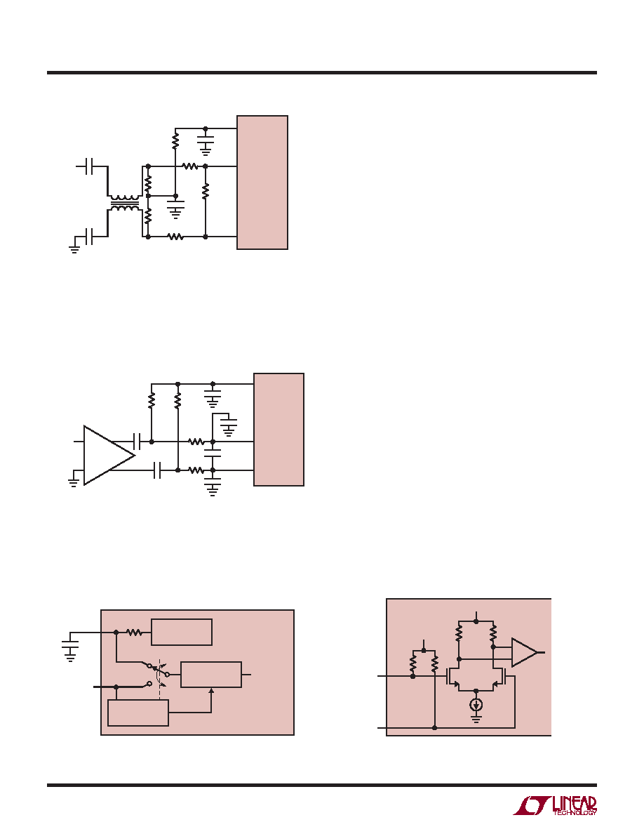
Figure 5. Recommended Front-End Circuit for
Input Frequencies from 150MHz to 900MHz
Figure 6. Front-End Circuit Using a High
Speed Differential Amplifier
Amplifier Circuits
Figure 6 shows the analog input being driven by a high
speed differential amplifier. The output of the amplifier is
AC coupled to the A/D so the amplifier’s output common
mode voltage can be optimally set to minimize distortion.
At very high frequencies an RF gain block will often have
lower distortion than a differential amplifier. If the gain
block is single-ended, then a transformer circuit (Figures
3 and 5) should convert the signal to differential before
driving the A/D. The A/D cannot be driven single-ended.
Reference
The LTC2158-14 has an internal 1.25V voltage reference.
For a 1.32V input range with internal reference, connect
SENSE to VDD. For a 1.32V input range with an external
reference, apply a 1.25V reference voltage to SENSE
(Figure 7).
Encode Input
The signal quality of the encode inputs strongly affects
the A/D noise performance. The encode inputs should
be treated as analog signals—do not route them next to
digital traces on the circuit board.
The encode inputs are internally biased to 1.2V through
10k equivalent resistance (Figure 8). If the common mode
of the driver is within 1.1V to 1.5V, it is possible to drive
the encode inputs directly. Otherwise a transformer or
coupling capacitors are needed (Figures 9 and 10). The
maximum (peak) voltage of the input signal should never
exceed VDD +0.1V or go below –0.1V.
4.7
50
0.1F
AIN+
AIN–
0.1F
3pF
VCM
LTC2158-14
215814 F06
INPUT
0.1F
45
10
100
4.7
0.1F
IN
0.1F
T1: MABA
007159-000000
215814 F05
LTC2158-14
AIN+
AIN–
VCM
Figure 7. Reference Circuit
Figure 8. Equivalent Encode Input Circuit
VDD
LTC2158-14
215814 F08
1.2V
10k
ENC+
ENC–
SCALER/
BUFFER
VREF
2.2F
SENSE
1.25V
LTC2158-14
215814 F07
5
ADC
REFERENCE
SENSE
DETECTOR
相关PDF资料 |
PDF描述 |
|---|---|
| LTC2172IUKG-14#TRPBF | IC ADC 14BIT SER/PAR 65M 52-QFN |
| LTC2175IUKG-14#TRPBF | IC ADC 14BIT 125MSPS QUAD 52QFN |
| LTC2202IUK#TRPBF | IC ADC 16-BIT 10MSPS 48-QFN |
| LTC2205IUK-14#PBF | IC ADC 14BIT 65MSPS 48-QFN |
| LTC2207IUK-14#PBF | IC ADC 14BIT 105MSPS 48-QFN |
相关代理商/技术参数 |
参数描述 |
|---|---|
| LTC2159 | 制造商:LINER 制造商全称:Linear Technology 功能描述:16-Bit, 20Msps Low Power ADC |
| LTC2159CUK#PBF | 功能描述:IC ADC 16BIT PAR/SRL 20M 48-QFN RoHS:是 类别:集成电路 (IC) >> 数据采集 - 模数转换器 系列:- 标准包装:1 系列:- 位数:14 采样率(每秒):83k 数据接口:串行,并联 转换器数目:1 功率耗散(最大):95mW 电压电源:双 ± 工作温度:0°C ~ 70°C 安装类型:通孔 封装/外壳:28-DIP(0.600",15.24mm) 供应商设备封装:28-PDIP 包装:管件 输入数目和类型:1 个单端,双极 |
| LTC2159CUK#TRPBF | 功能描述:IC ADC 16BIT PAR/SRL 20M 48-QFN RoHS:是 类别:集成电路 (IC) >> 数据采集 - 模数转换器 系列:- 标准包装:1 系列:- 位数:14 采样率(每秒):83k 数据接口:串行,并联 转换器数目:1 功率耗散(最大):95mW 电压电源:双 ± 工作温度:0°C ~ 70°C 安装类型:通孔 封装/外壳:28-DIP(0.600",15.24mm) 供应商设备封装:28-PDIP 包装:管件 输入数目和类型:1 个单端,双极 |
| LTC2159IUK#PBF | 功能描述:IC ADC 16BIT PAR/SRL 20M 48-QFN RoHS:是 类别:集成电路 (IC) >> 数据采集 - 模数转换器 系列:- 标准包装:1 系列:- 位数:14 采样率(每秒):83k 数据接口:串行,并联 转换器数目:1 功率耗散(最大):95mW 电压电源:双 ± 工作温度:0°C ~ 70°C 安装类型:通孔 封装/外壳:28-DIP(0.600",15.24mm) 供应商设备封装:28-PDIP 包装:管件 输入数目和类型:1 个单端,双极 |
| LTC2159IUK#TRPBF | 功能描述:IC ADC 16BIT PAR/SRL 20M 48-QFN RoHS:是 类别:集成电路 (IC) >> 数据采集 - 模数转换器 系列:- 标准包装:1 系列:- 位数:14 采样率(每秒):83k 数据接口:串行,并联 转换器数目:1 功率耗散(最大):95mW 电压电源:双 ± 工作温度:0°C ~ 70°C 安装类型:通孔 封装/外壳:28-DIP(0.600",15.24mm) 供应商设备封装:28-PDIP 包装:管件 输入数目和类型:1 个单端,双极 |
发布紧急采购,3分钟左右您将得到回复。